SLAA476B February 2011 – July 2019 BQ2040 , BQ2040 , BQ2060A , BQ2060A , BQ2063 , BQ2063 , BQ2083-V1P3 , BQ2083-V1P3 , BQ2084-V143 , BQ2084-V143 , BQ2084-V150 , BQ2084-V150 , BQ2085-V1P3 , BQ2085-V1P3 , BQ20Z40-R1 , BQ20Z40-R1 , BQ20Z70-V160 , BQ20Z70-V160 , BQ20Z80A-V110 , BQ20Z80A-V110 , BQ28400 , BQ28400 , BQ78PL114 , BQ78PL114 , BQ78PL116 , BQ78PL116 , LM5145 , LM5145 , MSP430F5500 , MSP430F5500 , MSP430F5501 , MSP430F5501 , MSP430F5502 , MSP430F5502 , MSP430F5503 , MSP430F5503 , MSP430F5504 , MSP430F5504 , MSP430F5505 , MSP430F5505 , MSP430F5506 , MSP430F5506 , MSP430F5507 , MSP430F5507 , MSP430F5508 , MSP430F5508 , MSP430F5509 , MSP430F5509 , MSP430F5510 , MSP430F5510 , TPS40057 , TPS40057 , TPS40170 , TPS40170
-
Wide-Vin Battery Charger Using SMBus Communication Interface Between MSP430™ MCUs and bq Fuel Gauges
- Trademarks
- 1 Introduction
- 2 Hardware
- 3
Software
- 3.1 SMBus Protocol Description
- 3.2 Software File Structure
- 3.3
API Calls Description
- 3.3.1 UCS_Init ( )
- 3.3.2 Timer_Init ( )
- 3.3.3 PWM_Init ( )
- 3.3.4 ADC_Init ( )
- 3.3.5 Fan_Init ( )
- 3.3.6 LED_Init ( )
- 3.3.7 SMBus_Initialize ( )
- 3.3.8 LED_Control ( )
- 3.3.9 Fan_Control ( )
- 3.3.10 VI_ADC_Read ( )
- 3.3.11 SMBus_Select ( )
- 3.3.12 Calibrate_Battery ( )
- 3.3.13 Delay_Timer ( )
- 3.3.14 PWM_Control ( )
- 3.3.15 Smbus_Access ( )
- 3.3.16 Smbus_Access_PEC ( )
- 3.3.17 crc8MakeBitwise ( )
- 3.4 Sample Application Description
- 4 SBS Supported Commands Using SMBus Protocol
- 5 Detailed Sample Application Flow Chart
- 6 Battery Status Register Description
- 7 MSP430F5510 Daughterboard Schematics
- 8 Setting Up the MSP430F5510 Daughterboard Hardware
- 9 Battery Calibration Circuit Setup
- 10 Battery Voltage and PWM Conversions
- 11 Battery Current and PWM Conversions
- 12 Power Stage Board Schematics (Generation 1: 40-V Input)
- 13 Bode Plot Measurement for Feedback Loop Stability Analysis
- 14 Power Stage Board Schematics (Generation 2: 60-V Input)
- 15 Setting Up the Power Stage Board Hardware
- 16 References
- Revision History
2.2.1 Subsystem Description
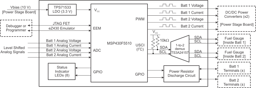
Figure 3 shows the block diagram of the MSP430F5510 daughterboard subsystem.
 Figure 3. MSP430F5510 Daughterboard Subsystem Block Diagram
 The daughtercard subsystem has the following features:
- The I2C USCI module within the MSP430F5510 is used to implement the SMBus protocol for communication with the battery fuel gauges.
- A 1-to-2 demultiplexer (demux), TS3A24157, is used to separate the SMBus clock (SCL) and data (SDA) lines for the two batteries [15]. During the manufacturing process, all of the fuel gauges for a particular battery series are programmed to the same SMBus slave address. The advantage of using a demux is that one microcontroller with one I2C/SMBus USCI module can be used to communicate with multiple fuel gauges within multiple smart-batteries.
- The MSP430F5510 outputs voltage and current PWM signals at a frequency of 20 kHz to control the power delivered by the DC/DC converters on the power stage subsystem.
- The on-chip 10-bit ADC is used to convert voltage and current signals from the batteries. The voltage from the battery is divided down from the wide-input range to the ADC range by means of a resistor-divider circuit on the MSP430F5510 daughterboard. The current is fed into a shunt resistor on the power-stage board, and the resulting voltage is fed into the ADC channels directly.
- Eight status LED indicators; seven are software programmable, and one indicates power-on status.
- Two sets of power resistors for discharging two batteries independently. The discharge circuitry can be turned on or off by the microcontroller to calibrate battery pack voltages. Section 9 has details on setting up these circuits.
- Fan control output to power a heat venting circulation fan on or off.
- Two options to program the software on the MSP430F5510 daughterboard:
- 14-pin JTAG interface (four-wire) for connecting the flash emulation tool (FET)
- 6-pin Spy-Bi-Wire interface (two-wire) for connecting the eZ430 emulator
- Three options to power the MSP430F5510 daughterboard:
- JTAG interface (voltage level programmable in the integrated development environment (IDE) options)
- eZ430 emulator interface (supply voltage fixed at 3.6 V)
- The charger board supply power (approximately 10 V), which is routed through the TPS71533 LDO to supply 3.3 V to the MSP430F5510 [16]. For a wider input supply range up to 50 V, the TPS79801 LDO can also be used to supply 3.3 V [17].