SLAAED5 june 2023 AFE11612-SEP , INA240-SEP , OPA4H199-SEP
- 1
- Abstract
- Trademarks
- 1 LDMOS and GaN Power Amplifier FET PA Basics
- 2 VGS Compensation
- 3 Sequencing
- 4 An Integrated PA Biasing Solution
- 5 Negative GaN Biasing
- 6 VDRAIN Switching Circuit
- 7 Controlled Gate Sequencing Circuit
- 8 VDRAIN Monitoring
- 9 IDQ Monitoring
- 10External Negative Power Supply Monitoring
- 11PA Temperature Monitoring
- 12Summary
- 13References
3 Sequencing
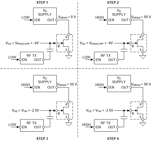
Powering the PA on and off in a controlled routine is necessary to prevent the VGS voltage from being too high when the VDRAIN is applied. Such a state causes the PA to operate in saturation mode which may result in thermal damage in the PA or the board it is mounted on. Powering on a PA requires the following steps:
- First, apply the VGS signal to the PA. The VGS voltage must transition to the VGS pinch-off voltage or lower. This ensures that when the VDRAIN voltage is applied, the gate is already low.
- Next, enable the drain voltage supply and allow the VDRAIN to be powered to the nominal value (50 V, for example). As the VGS is at the pinch-off voltage, IDS must be minimal.
- After the VDRAIN is applied, increase the VGS bias voltage to set the desired power output of the PA.
- Finally, enable the RF signal. This allows the PA to transmit a signal.
 Figure 3-1 GaN Power Sequencing
The PA can be safely shut down by reversing the power-on steps.
- Disable the RF signal from the PA.
- Reduce the VGS voltage to the pinch-off value, eliminating the power output of the PA.
- Disable the VDRAIN voltage by sending a disable signal to the drain supply.
- Finally, the VGS voltage can be allowed to collapse to ground as the PA is fully disabled.