SLAU678C March   2016  – November 2022


  1.   Abstract
  2.   Trademarks
  3. 1Getting Started
    1. 1.1 Introduction
    2. 1.2 Key Features
    3. 1.3 What's Included
      1. 1.3.1 Kit Contents
      2. 1.3.2 Software Examples
    4. 1.4 First Steps: Out-of-Box Experience
      1. 1.4.1 Connecting to the Computer
      2. 1.4.2 Running the Out-of-Box Demo
        1. 1.4.2.1 Live Temperature Mode
        2. 1.4.2.2 FRAM Data Log Mode
        3. 1.4.2.3 SD Card Data Log Mode
    5. 1.5 Next Steps: Looking Into the Provided Code
  4. 2Hardware
    1. 2.1 Block Diagram
    2. 2.2 Hardware Features
      1. 2.2.1 MSP430FR5994 MCU
      2. 2.2.2 eZ-FET Onboard Debug Probe With EnergyTrace++ Technology
      3. 2.2.3 Debug Probe Connection: Isolation Jumper Block
      4. 2.2.4 Application (or Backchannel) UART
      5. 2.2.5 Special Features
        1. 2.2.5.1 microSD Card
        2. 2.2.5.2 220-mF Super Capacitor
    3. 2.3 Power
      1. 2.3.1 eZ-FET USB Power
      2. 2.3.2 BoosterPack Plug-in Module and External Power Supply
      3. 2.3.3 Super Cap (C1)
        1. 2.3.3.1 Charging the Super Cap
        2. 2.3.3.2 Using the Super Cap
        3. 2.3.3.3 Disabling the Super Cap
    4. 2.4 Measure MSP430 Current Draw
    5. 2.5 Clocking
    6. 2.6 Using the eZ-FET Debug Probe With a Different Target
    7. 2.7 BoosterPack Plug-in Module Pinout
    8. 2.8 Design Files
      1. 2.8.1 Hardware
      2. 2.8.2 Software
    9. 2.9 Hardware Change Log
  5. 3Software Examples
    1. 3.1 Out-of-Box Software Example
      1. 3.1.1 Source File Structure
      2. 3.1.2 Out-of-Box Demo GUI
      3. 3.1.3 Power Up and Idle
      4. 3.1.4 Live Temperature Mode
      5. 3.1.5 FRAM Log Mode
      6. 3.1.6 SD Card Log Mode
    2. 3.2 Blink LED Example
      1. 3.2.1 Source File Structure
    3. 3.3 BOOSTXL-AUDIO Audio Record and Playback Example
      1. 3.3.1 Source File Structure
      2. 3.3.2 Operation
    4. 3.4 Filtering and Signal Processing With LEA Reference Design Example
      1. 3.4.1 Source File Structure
      2. 3.4.2 Operation
    5. 3.5 Emulating EEPROM Reference Design Example
      1. 3.5.1 Source File Structure
      2. 3.5.2 Operation
  6. 4Resources
    1. 4.1 Integrated Development Environments
      1. 4.1.1 TI Cloud Development Tools
        1. 4.1.1.1 TI Resource Explorer Cloud
        2. 4.1.1.2 Code Composer Studio Cloud
      2. 4.1.2 Code Composer Studio™ IDE
      3. 4.1.3 IAR Embedded Workbench for MSP430
    2. 4.2 LaunchPad Websites
    3. 4.3 MSPWare and TI Resource Explorer
    4. 4.4 FRAM Utilities
      1. 4.4.1 Compute Through Power Loss (CTPL)
    5. 4.5 MSP430FR5994 MCU
      1. 4.5.1 Device Documentation
      2. 4.5.2 MSP430FR5994 Code Examples
      3. 4.5.3 MSP430 Application Notes and TI Reference Designs
    6. 4.6 Community Resources
      1. 4.6.1 TI E2E Support Forums
      2. 4.6.2 Community at Large
  7. 5FAQ
  8. 6Schematics
  9. 7Revision History

FRAM Log Mode

To enter the FRAM Log Mode, click the Start button under FRAM Log Mode in the GUI Application Controls panel. The PC GUI also sends its current timestamp over UART to be stored in the LaunchPad development kit. This timestamp is later used to extrapolate the X-axis time values when the FRAM logged data are transferred to the GUI (see Figure 3-3).
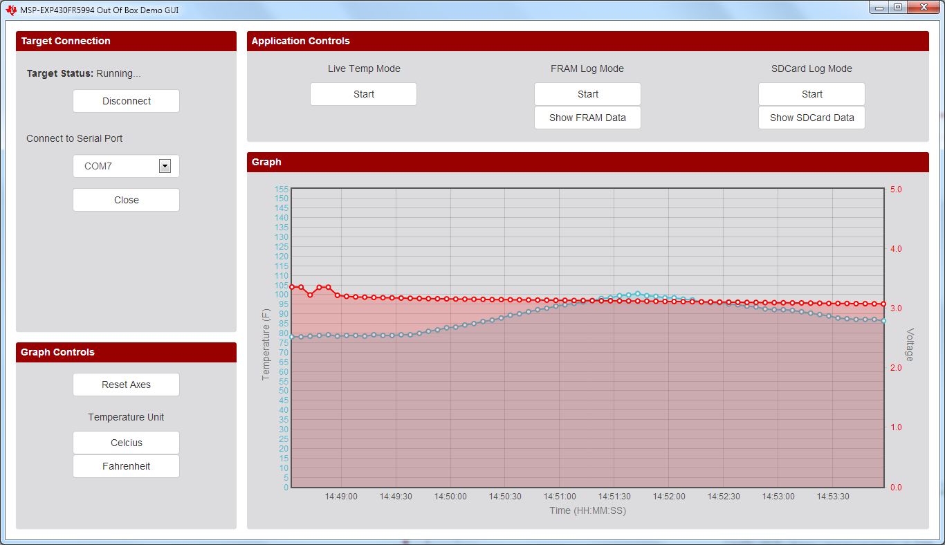
GUID-28CD45A3-D06B-49EA-9C21-E536BB3A998D-low.pngFigure 3-3 FRAM Log Mode

When the MSP430FR5994 receives the UART command from the GUI, it starts the entry sequence by initializing the Real-Time Clock to trigger an interrupt every 5 seconds. The red LED blinks three times to indicate successful entry into FRAM Log Mode.

The MSP430FR5994 wakes up every 5 seconds from low-power mode 3 to perform data logging before going back to low-power mode 3. The GUI automatically disconnects from the LaunchPad development kit after entering FRAM Log Mode. Each time the device wakes up, the green LED lights up to indicate a data point is stored. Two 10000 long FRAM array buffers are allocated to store the raw ADC output data.

Because the device can be powered solely with the onboard Super Cap, the 12-bit ADC is set up to sample and convert the signals from its internal temperature sensor and battery monitor (super cap voltage).

The board allows powering the application with the USB cable or the onboard super cap. See Section 2.3.3 for more detail on the super cap. To switch to the super cap:

  1. While board is powered through USB, configure the jumper to Charge on J8. Wait 2 to 3 minutes.
  2. Start FRAM Logging.
  3. Switch the jumper on J8 to Use.
  4. Disconnect the SBWTDIO and 3v3 jumpers on J101 (to prevent back powering the eZ-FET).
  5. Disconnect the USB.
Note:

Remove the SD card from the holder to reduce power consumption and extend application run time when using the super cap.

To exit the FRAM Log Mode, press the S2 (right) push button on the LaunchPad development kit. The red LED turns on briefly to indicate successful exit and return to the Power up and Idle state. Reattach the jumpers to the default positions and connect USB. Re-open the serial port to the LaunchPad development kit in the GUI. Click the Transfer FRAM Data button to transmit the logged temperature and voltage data from the device FRAM to the PC.