SLDU007C March   2012  – November 2015 PGA450-Q1


  1.   PGA450Q1EVM User’s Guide
    1.     Trademarks
    2. Read This First
    3. EVM Overview
    4. Power-Supply Requirements and Connections
      1. 3.1 Power Supply
      2. 3.2 Controlling and Powering the PGA450Q1EVM via the USB Interface Board
      3. 3.3 Connecting the Transducer
    5. Jumper Settings
      1. 4.1 Jumpers
      2. 4.2 Default Jumper Settings
      3. 4.3 0-Ω Resistors
    6. Socket for Programming OTP
    7. Transformer and Transducer
    8. PGA450-Q1 Communication Interfaces
      1. 7.1 SPI
      2. 7.2 LIN
      3. 7.3 UART
    9. Controlling the PGA450-Q1 Memory Spaces With the GUI
      1. 8.1 Using the Register Grids to Manipulate the Register Spaces
        1. 8.1.1 ZERO GRID
        2. 8.1.2 DESELECT GRID
        3. 8.1.3 SAVE GRID
        4. 8.1.4 RECALL GRID
        5. 8.1.5 READ SELECTED
        6. 8.1.6 WRITE SELECTED
        7. 8.1.7 READ ALL
        8. 8.1.8 WRITE ALL
      2. 8.2 ESFR Registers
      3. 8.3 EEPROM Registers
        1. 8.3.1 Program EEPROM
        2. 8.3.2 Reload EEPROM
      4. 8.4 RAM
      5. 8.5 OTP
        1. 8.5.1 Load .HEX File Into GUI
        2. 8.5.2 Program OTP Memory from .HEX File
        3. 8.5.3 Verify OTP Programming
        4. 8.5.4 Check OTP Status
      6. 8.6 DEVRAM
      7. 8.7 FIFO/ECHO
        1. 8.7.1 FIFO
        2. 8.7.2 EVAL Monitor
          1. 8.7.2.1 No. of Loops
          2. 8.7.2.2 Trigger
          3. 8.7.2.3 Resolution
          4. 8.7.2.4 Clear Plot
          5. 8.7.2.5 Export Data to Excel
          6. 8.7.2.6 Start/Stop
    10. LIN Master
    11. 10 Keil uVision Settings for Programming Firmware to the PGA450-Q1 DEVRAM or OTP Memory
      1. 10.1 Objective
      2. 10.2 Setup
    12. 11 Use Case
      1. 11.1 Evaluation Through SPI Communication
      2. 11.2 Monitoring the Signal Path
    13. 12 PGA450Q1EVM Schematics and Layout Drawings
  2.   Revision History

DEVRAM

The DEVRAM tab is set up only for individual register read/writes, without the use of the grid. When this tab is displayed, the READ SELECTED / READ ALL and WRITE SELECTED / WRITE ALL buttons perform the same operations, respectively. The DEVRAM tab also contains buttons used to load a .HEX 8051 program file into the 8051 MCU in the PGA450-Q1 device.

The process of loading the .HEX file into the DEVRAM is identical to that of OTP.

For a pristine IC that has never been programmed (OTP Status reads "OTP Empty"), in order to run software from DEVRAM, the OTP memory must be programmed with some specific instructions to redirect the 8051 µP to DEVRAM. This must only be done once. To do this, check the "Program OTP Memory Also" button, and the GUI will program the OTP with this jump statement as well as program the DEVRAM with the selected HEX file.
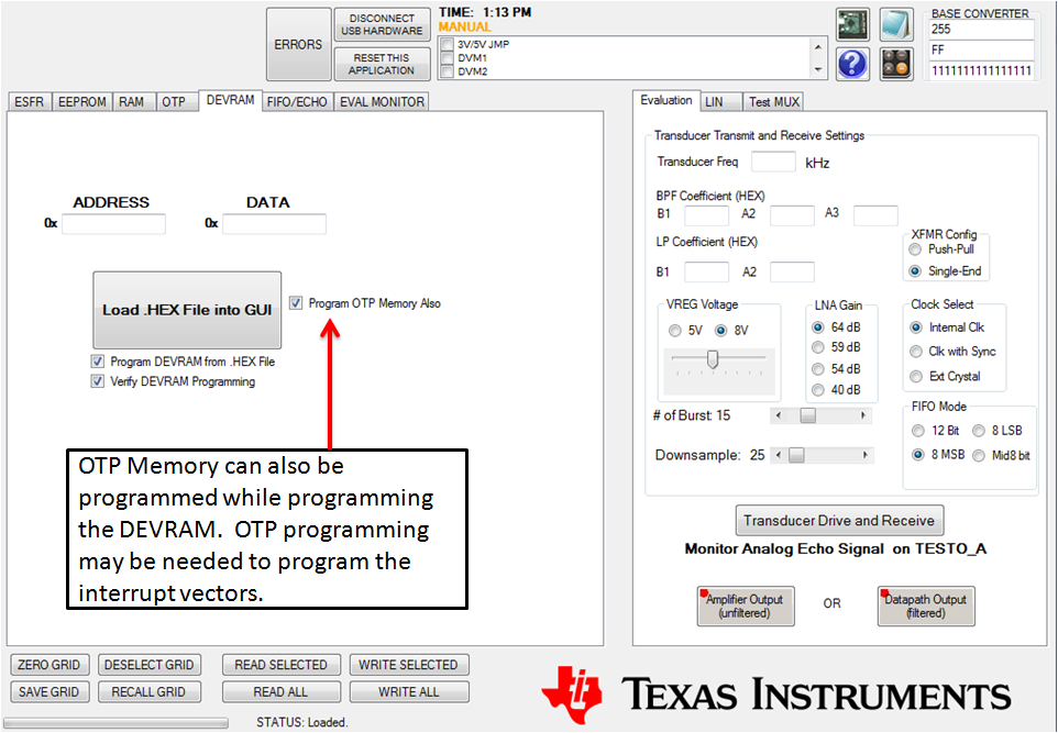
figure8_OTP_memory_program_sdlu007.png
Note that OTP programming may be required if the interrupt vectors are not programmed
Figure 8. OTP Memory can be programmed while programming the Development RAM