SLDU007C March 2012 – November 2015
-
PGA450Q1EVM User’s Guide
- Trademarks
- 1 Read This First
- 2 EVM Overview
- 3 Power-Supply Requirements and Connections
- 4 Jumper Settings
- 5 Socket for Programming OTP
- 6 Transformer and Transducer
- 7 PGA450-Q1 Communication Interfaces
- 8 Controlling the PGA450-Q1 Memory Spaces With the GUI
- 9 LIN Master
- 10 Keil uVision Settings for Programming Firmware to the PGA450-Q1 DEVRAM or OTP Memory
- 11 Use Case
- 12 PGA450Q1EVM Schematics and Layout Drawings
- Revision History
9 LIN Master
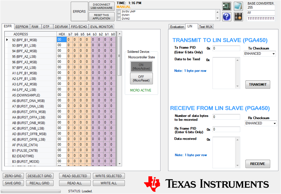
The PGA450Q1EVM GUI communicates with the PGA450-Q1 device using LIN. The USB Communication board UART is the LIN master, and the PGA450-Q1 device is the LIN slave. The GUI can be used to configure the LIN frames that are transmitted to the PGA450-Q1 device.
 Figure 10. LIN Master on GUI
 In order to transmit data to PGA450-Q1 device using a LIN frame, the user must do the following:
- Enter the Frame PID in Edit Box corresponding to “Tx Frame PID”. The PID must be entered in hex. Note that valid PID ranges from 0x00 to 0x3F. The GUI software calculates the parity bits using the LIN 2.1 method before the PID is transmitted to the slave.
- Enter 0–8 bytes of data in the “Data to be Txed” box. Each data byte must be entered in Hex.
- Select the CLASSIC or ENHANCED checksum, which must match the LIN checksum setting in the PGA450-Q1 ESFR LIN_CFG register.
- Click on the TRANSMIT button
In order to receive data from PGA450-Q1 device using a LIN frame, the user must do the following:
- Enter the Frame PID in Edit Box corresponding to “Rx Frame PID”. The PID must be entered in hex. Note that valid PID ranges from 0x00 to 0x3F. The GUI software calculates the parity bits using the LIN 2.1 method before the PID is transmitted.
- Enter the number of data bytes the user expects back from the PGA450-Q1 device.
- Select the CLASSIC or ENHANCED checksum
- Click on the RECEIVE button
The data received from the PGA450-Q1 device is displayed in the Data Received box.
If the data communication is not working, try Reset This Application, which power-cycles the LIN master IC on the EVM.