SLOA277B january   2019  – july 2023 LM124 , LM124-N , LM124A , LM158 , LM158-N , LM158A , LM224 , LM224-N , LM224A , LM258 , LM258-N , LM258A , LM2902 , LM2902-N , LM2902-Q1 , LM2902K , LM2902KAV , LM2904 , LM2904-N , LM2904-Q1 , LM2904B , LM2904B-Q1 , LM2904BA , LM321 , LM324 , LM324-N , LM324A , LM358 , LM358-N , LM358A , LM358B , LM358BA , TS321 , TS321-Q1


  1.   1
  2.   Abstract
  3.   Trademarks
  4. 1Devices Covered in Application Note
    1. 1.1 Common Schematic
    2. 1.2 Base Part Numbers
    3. 1.3 Input Voltage Offset Grades
    4. 1.4 Maximum Supply Voltage
    5. 1.5 High Reliability Options
    6. 1.6 HBM ESD Grade
    7. 1.7 LM358B, LM358BA, LM2904B, LM2904BA, LM324B, LM2902B
  5. 2Input Stage Considerations
    1. 2.1 Input Stage Schematic
    2. 2.2 Input Common Mode Range
    3. 2.3 Input Impedance
    4. 2.4 Phase Reversal
  6. 3Output Stage Considerations
    1. 3.1 Output Stage Schematic, VOL and IOL
    2. 3.2 IOL and Common Mode Voltage
    3. 3.3 Output Stage Schematic, VOH and IOH
    4. 3.4 Short Circuit Sourcing Current
    5. 3.5 Output Voltage Limitations
  7. 4AC Performance
    1. 4.1 Slew Rate and Bandwidth
    2. 4.2 Slew Rate Variability
    3. 4.3 Output Crossover Time Delay
    4. 4.4 First Crossover Example
    5. 4.5 Second Crossover Example
  8. 5Low VCC Guidance
    1. 5.1 Low VCC Input Range Supporting –40°C
    2. 5.2 Low VCC Output Range Supporting –40°C
    3. 5.3 Low VCC Audio Amplifier Example
  9. 6Comparator Usage
    1. 6.1 Op Amp Limitations
    2. 6.2 Input and Output Voltage Ranges
    3. 6.3 Overload Recovery
    4. 6.4 Slew Rate
  10. 7Unused Amp Connections and Inputs Connected Directly to Ground
    1. 7.1 Do Not Connect Inputs Directly to Ground
    2. 7.2 Unused Amplifier Connections
  11. 8Conclusion
  12. 9Revision History

Second Crossover Example

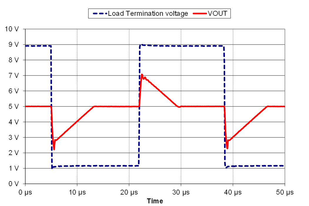
Crossover can also occur when the load current changes from an external source as seen in Figure 4-7. The LM358 is set up as a reference voltage buffer and the load current alternates between 1 mA and –1 mA.

GUID-712D4995-6A9D-4BFA-AC40-B903A1621E54-low.gifFigure 4-7 Second Crossover Test Schematic

The LM358 load current is stepped ±1 mA using a pulse generator square wave and a series resistor. Ideally, the output voltage should be constant at 5 V. However the output voltage jumps by 2 V, or about 3 × VBE, before the other output driver can provide current flow. At 25°C, the time needed to correct the output signal back to 5 V is about

Equation 2. 2   V 0 . 3   V / µs   =   6 . 7   µs

The LM358 has a slower typical slew rate than the LM324. Consequently, the time delay is greater in the LM358. The oscilloscope capture in Figure 4-8 shows as example output waveform in red and a pulse generator output in dotted blue. From this real-world data, we see that output crossover can create output steps and flat waveforms followed by a correction period.
GUID-7279F827-D111-4FAA-9018-FFED4138859B-low.gif Figure 4-8 LM358 Crossover Test Waveforms