SLOA277B january 2019 – july 2023 LM124 , LM124-N , LM124A , LM158 , LM158-N , LM158A , LM224 , LM224-N , LM224A , LM258 , LM258-N , LM258A , LM2902 , LM2902-N , LM2902-Q1 , LM2902K , LM2902KAV , LM2904 , LM2904-N , LM2904-Q1 , LM2904B , LM2904B-Q1 , LM2904BA , LM321 , LM324 , LM324-N , LM324A , LM358 , LM358-N , LM358A , LM358B , LM358BA , TS321 , TS321-Q1
3.1 Output Stage Schematic, VOL and IOL
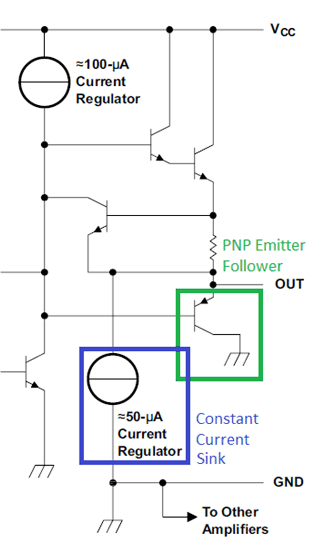
The op amp can provide a low output voltage near the negative rail, provided that the load and load termination voltage are aiding the ‘Constant Current Sink’ driver shown in Figure 3-1. Table 3-1 states that the output low voltage is less than 20 mV with a 10-kΩ or less load, assuming the negative supply is at GND. Therefore, if the load resistor is 10 kΩ or less and is terminated to the negative rail, then the load resistor helps the “Constant Current Sink” provide a very low output voltage.
| Parameter | Test Conditions | Typical | Maximum |
|---|---|---|---|
| VOL Low-Level Output Voltage | RL ≤ 10 kΩ | 5 mV | 20 mV |
If the op amp load, including the feedback network, is terminated to a positive voltage, then the op amp must sink current when driving the output low. The output stage seen in Figure 3-1 has a weak constant current sink consisting of a current regulator that provides a low output voltage for low levels of sink current. The PNP emitter follower can provide a much higher sink current at a higher output voltage.
 Figure 3-1 Schematic of Output Driver Stage With Highlighted Sink Drivers
The output pin can sink over 12 µA and still have a less than 200-mV output low level as seen in Table 3-2. From the electrical characteristics table in the data sheet, the typical output current is 30 µA or 40 µA. The "~50µA Current Regulator" in the device schematic is called a “constant current sink” driver in this application note because the current value is not necessarily 50 µA, as per the electrical characteristics table. Note that the data sheet specification has no maximum limit.
| Parameter | Test Conditions | Minimum | Typical |
|---|---|---|---|
| IO Output Current | VID = 1 V < VO = 200 mV | 12 µA | 40 µA |
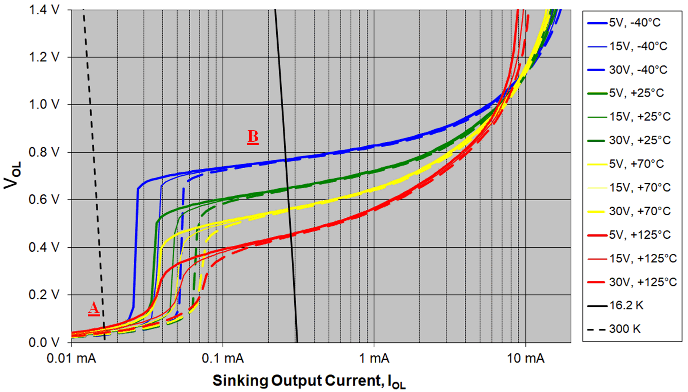
The output low voltage is less than 200 mV when sinking up to 12 µA. At higher current levels, the constant current sink is no longer sufficient. So, the PNP emitter follower supplies this current. However, no current is provided by the PNP emitter follower until the output voltage is approximately 600 mV, assuming room temperature. Note that when the PNP emitter follower is active, the VOL level has a temperature coefficient of approximately –2 mV/°C. The PNP emitter follower provides a low output impedance and the base current flows to the output load for a higher efficiency.
Figure 3-2 plots the low output voltage level vs the sinking current. As can be seen, there is an obvious transition from the constant sink driver (region "A") to the PNP emitter follower (region "B"). Note that the constant sink driver, as its name suggests, is always on.
 Figure 3-2 Typical Output Low Voltage vs
Output Sinking Current
Figure 3-2 Typical Output Low Voltage vs
Output Sinking CurrentIn Figure 3-2, two example load lines, a 16-kΩ (solid black line) resistor line and 300-kΩ (dotted black line) resistor line, are shown terminated to 5 V. The 300-kΩ load line intersects the device performance curves at a low VOL level across supply voltage and temperature. Therefore, a low VOL can be expected for this load. The 16-kΩ load line intersects the device performance curves at a higher VOL that varies with temperature, but not with VCC. With this load, a VOL near the negative supply is not possible. If having a low VOL is important, use high resistance loads or loads (including feedback) terminated to the negative supply.