SLUP412 February 2022 LMG3522R030-Q1
- 1 Introduction
- 2 Comparing Different Technologies
- 3 Advantages of Integrating the Driver With GaN FETs
- 4 The GaN-Based 6.6-kW OBC Reference Design
- 5 PFC Stage
- 6 DC/DC Stage
- 7 DC/DC Topology Selection
- 8 Frequency Selection
- 9 Core Loss
- 10Loss of ZVS
- 11Dead Time
- 12ISR Bandwidth
- 13Overall
- 14Resonant Tank Design
- 15Thermal Solution
- 16Layout Best Practices
- 17Control-Loop Considerations
- 18Conclusions
- 19References
- 20Important Notice
1 Introduction
The first generations of onboard chargers (OBCs) leveraged insulated gate bipolar transistors (IGBTs) and were huge and bulky. Figure 1-1 illustrates the improvement in solution size with better technologies and thermal concepts.
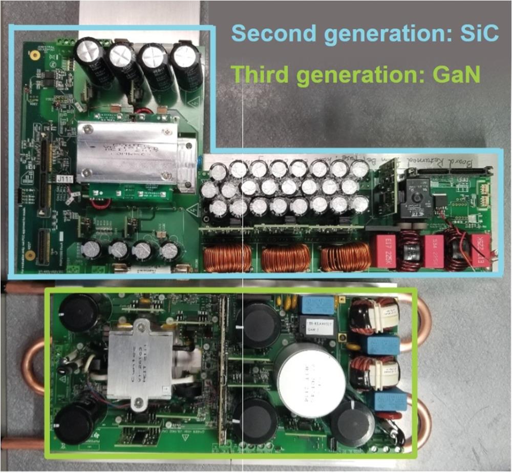 Figure 1-1 Second-generation SiC-based OBC
reference designs [1] (light-blue frame, convection-cooled) and a third-generation
GaN-based OBC reference design (green frame, liquid-cooled).
Figure 1-1 Second-generation SiC-based OBC
reference designs [1] (light-blue frame, convection-cooled) and a third-generation
GaN-based OBC reference design (green frame, liquid-cooled).GaN’s ultra-fast switching slew rates and liquid-cooled thermal interface yield a 22% reduction in size (area: 38,171 mm2) [2] compared to the convection-cooled SiC-based DC/DC and power factor correction (PFC) reference designs on the left [3] and right [4] inside the light-blue frame in Figure 1-1, respectively. Texas Instruments (TI) had designed these latter two reference designs (area: 27,886 mm2 + 20,915 mm2) three years earlier than the reference design in the green frame. This topic explains the design process behind the GaN-based reference design in the green frame.