SLUP412 February 2022 LMG3522R030-Q1
- 1 Introduction
- 2 Comparing Different Technologies
- 3 Advantages of Integrating the Driver With GaN FETs
- 4 The GaN-Based 6.6-kW OBC Reference Design
- 5 PFC Stage
- 6 DC/DC Stage
- 7 DC/DC Topology Selection
- 8 Frequency Selection
- 9 Core Loss
- 10Loss of ZVS
- 11Dead Time
- 12ISR Bandwidth
- 13Overall
- 14Resonant Tank Design
- 15Thermal Solution
- 16Layout Best Practices
- 17Control-Loop Considerations
- 18Conclusions
- 19References
- 20Important Notice
3 Advantages of Integrating the Driver With GaN FETs
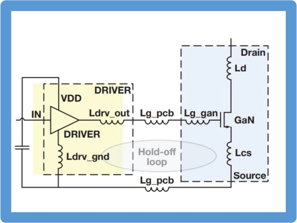
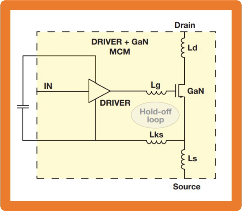
Two types of parasitic inductance between the driver and the FET limit the ultra-fast switching performance of GaN FETs: the common source inductance (CSI) and the gate-loop inductance. Minimizing both parasitic elements will help achieve the best possible switching performance.
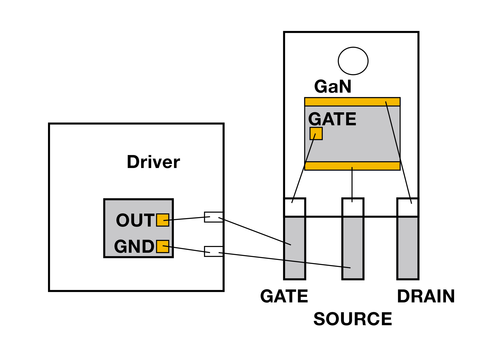
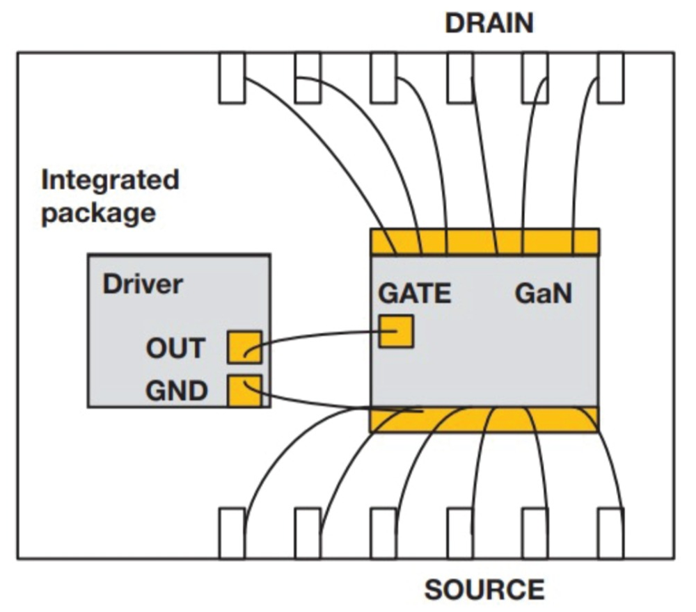
A completely discrete approach will result in a large CSI because of inductance contributions from the integrated circuit (IC) packages and the driver to FET routing distance on the printed circuit board (PCB). The result will cause slower turnon of the GaN FET, with increased losses. Most GaN FET manufacturers currently only offer packages with a separate Kelvin source connection to reduce the CSI. A discrete FET solution with an external gate driver will have a larger CSI compared to the integrated driver and GaN solution from TI (see Figure 3-1 through Figure 3-4).
 Figure 3-1 Discrete GaN FET and
driver.
 Figure 3-2 Discrete GaN FET and
equivalent circuit diagram.
 Figure 3-3 TI GaN FET with integrated
driver.
 Figure 3-4 TI GaN FET with equivalent
circuit diagram.
Figure 3-4 TI GaN FET with equivalent
circuit diagram.Meanwhile, integrating the driver and GaN also minimizes the gate-loop inductance, helping reduce gate-loop ringing, mitigating crosstalk, and improving gate reliability [6][7][8].
Figure 3-5 shows the simulated turnon switching waveforms of the high-side FET in a GaN FET half bridge for two different CSI values (0 nH and 5 nH).
Having the smallest possible CSI enables the GaN FET to turnon much faster, without causing any switch-node ringing. In addition, the turnon switching losses of the GaN FET are smaller with a lower CSI value, which helps improve system efficiency (see Figure 3-6).
There is a similar effect for the parasitic gate-loop inductance. Figure 3-7 illustrates that the smaller the gate-loop inductance value, the smaller the energy required to turnon the GaN FET (2 nH and 10 nH).