SLUP412 February 2022 LMG3522R030-Q1
- 1 Introduction
- 2 Comparing Different Technologies
- 3 Advantages of Integrating the Driver With GaN FETs
- 4 The GaN-Based 6.6-kW OBC Reference Design
- 5 PFC Stage
- 6 DC/DC Stage
- 7 DC/DC Topology Selection
- 8 Frequency Selection
- 9 Core Loss
- 10Loss of ZVS
- 11Dead Time
- 12ISR Bandwidth
- 13Overall
- 14Resonant Tank Design
- 15Thermal Solution
- 16Layout Best Practices
- 17Control-Loop Considerations
- 18Conclusions
- 19References
- 20Important Notice
14 Resonant Tank Design
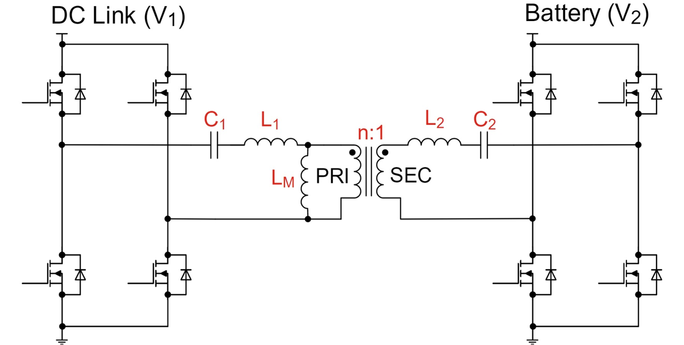
After selecting the operating frequency, we needed to determine six tank elements, shown in the highlighted boxes in Figure 14-1. Although the procedure we are about to describe will create a very reasonable starting point, it will not provide an exact solution. In general, it is difficult, if not impossible, to come up with an exact solution without detailed simulation and analysis. Real hardware always reveals subtleties not evident in the design phase. Still, it is almost always helpful to get to a reasonable starting point quickly, from which you can fine-tune a design as necessary through simulation and then hardware.
 Figure 14-1 CLLLC essential
parameters.
Figure 14-1 CLLLC essential
parameters.The design of the tank elements will have a profound effect on converter efficiency, thermal performance and size. Our primary considerations included:
- Core losses:
- Impacted by frequency, turns ratio and core size.
- Winding losses:
- The tank elements determine the winding currents.
- Inductances may drive larger gaps that can induce more losses caused by fringing.
- FET conduction losses:
- The tank elements determine the FET current.
- Maintaining ZVS:
- The tank current (and in particular the magnetizing inductance) determine whether it’s possible to maintain ZVS.
- Magnetics integration:
- Only realistic ratios of leakage inductance to magnetizing inductance can make magnetics integration physically realizable.
Consider the gain required in order to supply the necessary output voltage and current during charging and discharging. Both the turns ratio (n) and the magnetizing inductance (LM) have the largest influence on the required gains. The best designs often require iteration to see which combination yields the highest efficiency. It usually makes sense to start with n, since it has a bigger influence than LM.
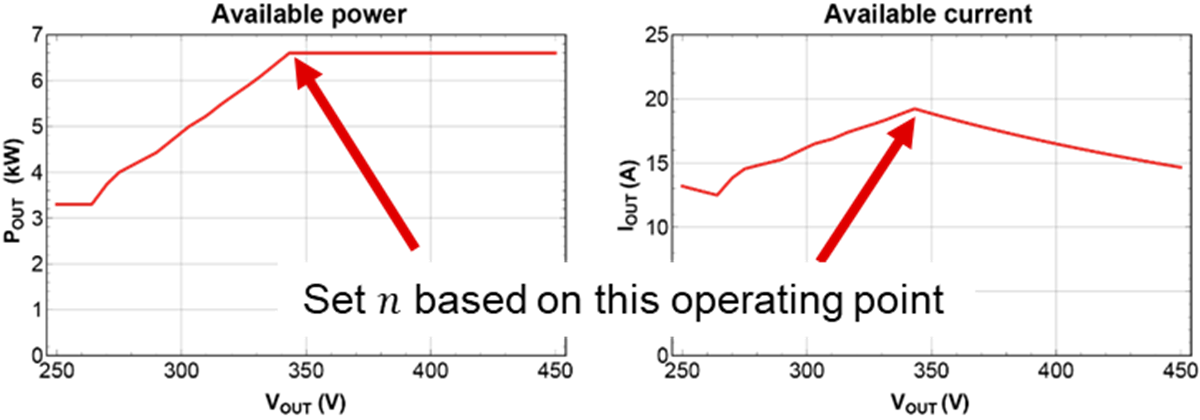
Resonant converters are most efficient when operating at or near the resonant frequency. Battery-charger requirements dictate that the converter charge with as much power or current as possible, meaning that the required current will be greatest when the output voltage is at its lowest. Choose n such that the converter operates with the lowest tank current possible when the required charge current is greatest. The converter will then operate close to resonance, and most importantly at its highest efficiency.
Figure 14-2 illustrates the operating point for the design where the secondary current is largest. This point dictates how to choose n.
 Figure 14-2 Turns ratio selection.
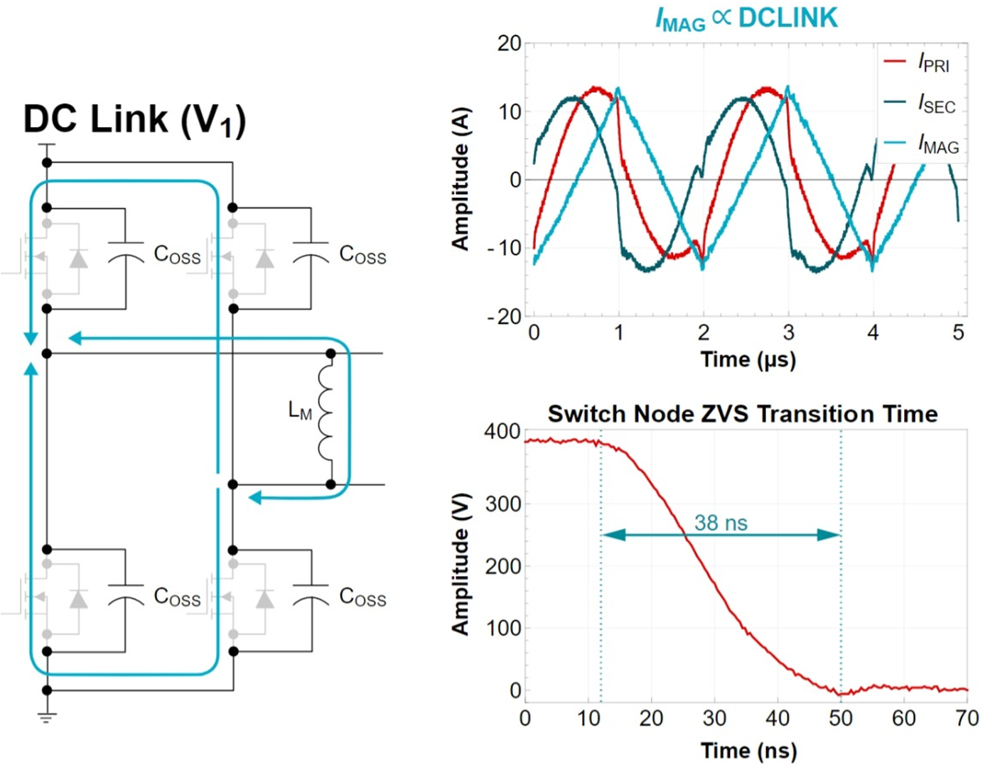
While LM affects both ZVS and gain, look at its impact on ZVS. Equation 3 through Equation 7 quantify the behavior during the switching transient, illustrated in Figure 14-3.
Equation 3 is the basic differential equation that defines how the magnetizing current evolves with time during a one-half cycle of switching:
where VDC_LINK is the converter input voltage and is the magnetizing current.
Since the applied voltage is constant, it is possible to simplify Equation 3 to Equation 4:
where is the change in the magnetizing current during a one-half cycle.
Equation 5 is the differential equation that defines how the GaN FET VDS will evolve over time. A common assumption is that is a constant during the dead time, but this is in fact not true. Making this assumption, however, will get you to a reasonable starting point.
where VDS(t) is the GaN FET VDS.
Since the current driving the FET is one-half the total delta, you can simplify Equation 5 to Equation 6:
where td is the dead time.
Simultaneously solving Equation 5 and Equation 6 results in Equation 7 – the LM that will facilitate ZVS in the targeted dead time:
where TS is the switching period.
 Figure 14-3 ZVS considerations.
Figure 14-3 illustrates the path that the current takes in the LM to charge and discharge the COSS capacitances of the GaN FETs. The measured waveforms show the primary, secondary and magnetizing currents. The switch-node transition time achieved with a 14-µH LM was 38 ns.
As a side note, Equation 3 through Equation 7 predict an LM value of 20 µH. 14 µH was used in order to better enhance ZVS over a wider range of operating points and help achieve the necessary gain.
Then, first harmonic analysis (FHA) was used to assess the converter’s overall ability to meet the charge and discharge profiles. Figure 14-4 illustrates the method. Essentially, replacing the switch networks with sinusoidal equivalents makes it possible to analyze the tank elements using classic S-domain frequency analysis.
 Figure 14-4 FHA method.
From here, some assumptions were made to reduce the number of variables. First, that the inductance on both sides of the isolation barrier is equivalent through the turns ratio. Mathematically, this means .
Next, the capacitance ratio was set, , such that . This means that m = 1.
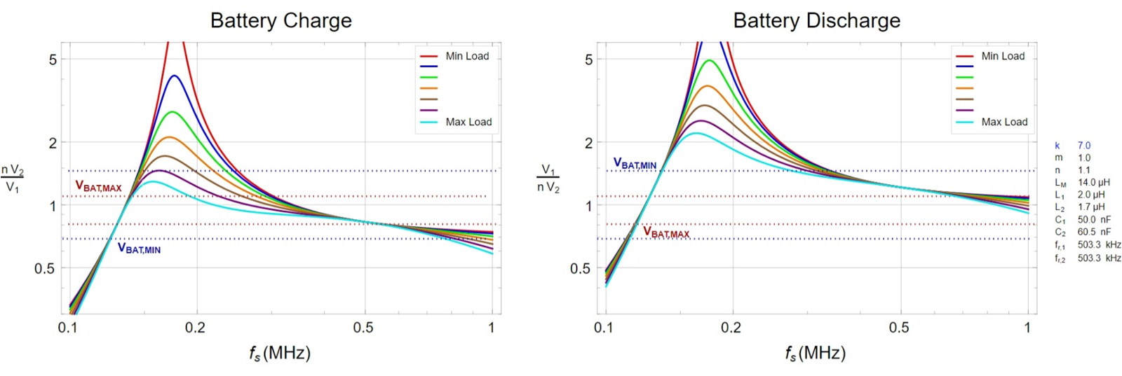
With these assumptions, all that remains is to select the ratio, , which will adjust the tank gain such that it is possible to meet the charge and discharge profiles. Plotting the charge and discharge curves for various values of k and selecting the design point that best maps to the required gain will determine k. Figure 14-5 illustrates the values.
 Figure 14-5 FHA gain curves.