SLUP412 February 2022 LMG3522R030-Q1
- 1 Introduction
- 2 Comparing Different Technologies
- 3 Advantages of Integrating the Driver With GaN FETs
- 4 The GaN-Based 6.6-kW OBC Reference Design
- 5 PFC Stage
- 6 DC/DC Stage
- 7 DC/DC Topology Selection
- 8 Frequency Selection
- 9 Core Loss
- 10Loss of ZVS
- 11Dead Time
- 12ISR Bandwidth
- 13Overall
- 14Resonant Tank Design
- 15Thermal Solution
- 16Layout Best Practices
- 17Control-Loop Considerations
- 18Conclusions
- 19References
- 20Important Notice
2 Comparing Different Technologies
Table 2-1 compares the parameters of silicon/IGBT, SiC and GaN devices. The reason why the vast majority of designs use silicon is because silicon still has a cost advantage over wide-bandgap devices. This gap will likely become smaller in the near future.
| Parameter | Silicon/IGBT | SiC | TI GaN |
|---|---|---|---|
| RDS(on) | High | Medium | Low |
| VDS | Up to several kilovolts | 650 V/900 V/ 1,200 V/1,700 V |
600 V/650 V |
| Maximum operating fsw | Low | Medium | High |
| Qrr | High | Low | Zero |
| Tj,max | 150°C/175°C | 175°C/200°C | 150°C |
| Thermal Conductivity | 1.5 W/(cm × K) | 5 W/(cm × K) | 1.3 W/(cm × K) |
| Cost | Low | High | Medium |
Wide-bandgap devices come into play when the design calls for the transfer of high power in a specified form factor and silicon-based solutions reach their thermal limits, either generating too many losses or requiring too many semiconductor components in parallel to keep the losses at bay, which can lead to a more expensive overall solution.
GaN high-electron mobility transistors enable designers to reach higher power density levels than any other technology on the market. Their parasitic elements are smaller compared to silicon and SiC devices, allowing switching at higher frequencies with acceptable losses. Direct drive of TI GaN FETs results in a zero reverse-recovery charge characteristic, which is beneficial for hard-switched continuous conduction mode (CCM) topologies such as the CCM totem-pole PFC converter [5]. CCM totem-pole PFC converters with silicon switches have never been viable given the immense losses caused by the large reverse-recovery charge of silicon metal-oxide semiconductor field-effect transistors (MOSFETs).
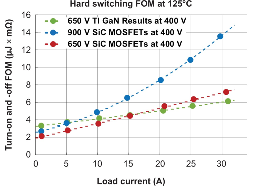
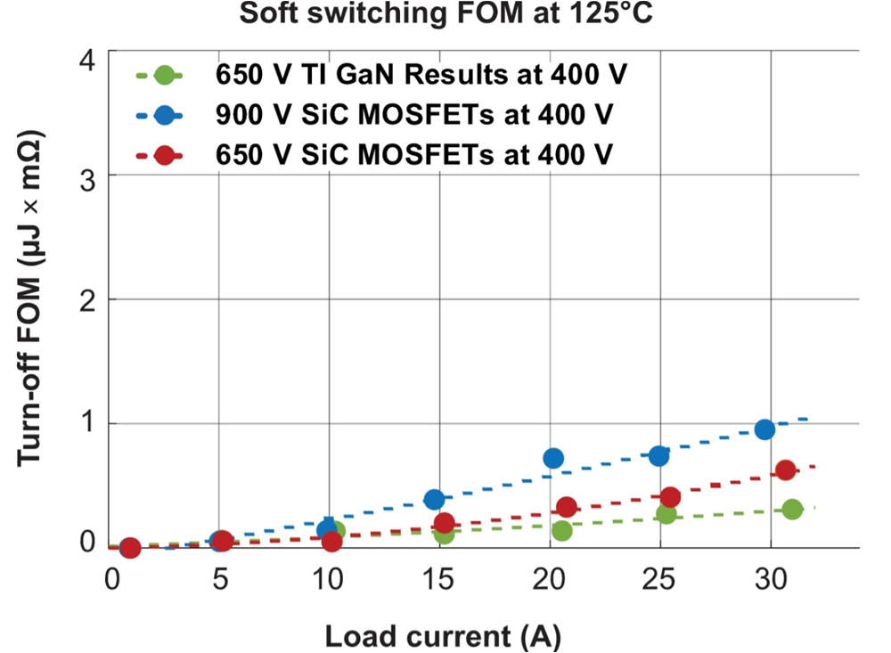
Writing this paper called for a performance comparison between SiC MOSFETs and GaN. To accurately compare TI GaN devices with ultra-fast slew rates (>150 V/ns), you would need to consider SiC MOSFETs in a low-inductance package with fast-switching-speed capability. In the commercial market, however, SiC FETs with similar RDS(on) and voltage ratings are not readily available in a low-inductance package with a Kelvin source connection. So instead, SiC FETs with a larger RDS(on) were tested and used the switching figure-of-merit (FOM) concept for both hard- and soft-switching comparisons, as shown in Figure 2-1 and Figure 2-2.
 Figure 2-1 Hard-switching FOM comparison
of SiC and TI GaN.
 Figure 2-2 Soft-switching FOM comparison
of SiC and TI GaN.
Figure 2-2 Soft-switching FOM comparison
of SiC and TI GaN.From the FOM graphs, you can see that under soft switching, TI GaN has an immense advantage over SiC MOSFETs, with significantly lower turnoff losses as a result of the direct-drive approach. In hard-switching conditions, the total switching loss includes both turnon and turnoff energy losses. The overall switching losses are proportional to the product of the switching frequency and energy required to turn the respective FET on and off. Equation 1 expresses this relationship:
The hard-switching FOM shows that TI GaN generates fewer losses at load currents greater than 15 A and is a better fit for high-current applications.