SLUSAM9E July 2011 – April 2020 BQ76925
PRODUCTION DATA.
- 1 Features
- 2 Applications
- 3 Description
- 4 Revision History
- 5 Description (Continued)
- 6 Pin Configuration and Functions
-
7 Specifications
- 7.1 Absolute Maximum Ratings
- 7.2 ESD Ratings
- 7.3 Recommended Operating Conditions
- 7.4 Thermal Information
- 7.5 Electrical Characteristics: Supply Current
- 7.6 Internal Power Control (Startup and Shutdown)
- 7.7 3.3-V Voltage Regulator
- 7.8 Voltage Reference
- 7.9 Cell Voltage Amplifier
- 7.10 Current Sense Amplifier
- 7.11 Overcurrent Comparator
- 7.12 Internal Temperature Measurement
- 7.13 Cell Balancing and Open Cell Detection
- 7.14 I2C Compatible Interface
- 7.15 Typical Characteristics
-
8 Detailed Description
- 8.1 Overview
- 8.2 Functional Block Diagram
- 8.3 Feature Description
- 8.4 Device Functional Modes
- 8.5 Programming
- 8.6 Register Maps
- 9 Application and Implementation
- 10Power Supply Recommendations
- 11Layout
- 12Device and Documentation Support
- 13Mechanical, Packaging, and Orderable Information
8.3.2.2.2 Cell Amplifier Headroom Under BAT Voltage Drop
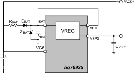
Voltage differences between BAT and the top cell potential come from two sources as shown in Figure 11: V3P3 regulator current that flows through the RBAT filter resistor, and the voltage drop in the series diode DBAT of the hold-up circuit. These effects cause BAT to be less than the top-cell voltage measured by the cell amplifier.
 Figure 11. Sources of Voltage Drop Affecting the BAT Pin
 The top-cell amplifier (VC6 – VC5) is designed to measure an input voltage down to 1.4 V with a difference between the BAT and VC6 pin up to 1.2 V (that is, BAT can be 1.2 V lower than VC6). However, in applications with fewer than 6 cells, the upper-cell inputs are typically shorted to the top-cell input. For example, in a 5-cell application VC6 and VC5 would be shorted together and the (VC5 – VC4) amplifier would measure the top-cell voltage. The case is similar for 4-cell and 3-cell applications.
For these cases when using the (VC5 – VC4), (VC4 –VC3), or (VC3 – VC2) amplifier to measure the top cell, the difference between BAT and the top-cell amplifier must be less than 240 mV in order to measure cell voltages down to 1.4 V. Note that at higher-cell input voltages the top amplifier tolerates a greater difference. For example, in a 5-cell configuration (VC6 and VC5 tied together) the (VC5 – VC4) amplifier is able to measure down to a 1.7 V input with a 600-mV difference between VC5 and BAT.
Accordingly, in systems with fewer than 6 cells, it is important in system design to minimize RBAT and to use a Schottky type diode for DBAT with a low forward voltage. If it is not possible to reduce the drop at BAT to an acceptable level, then for 4-cell and 5-cell configurations, the (VC6 – VC5) amplifier may be used as the top cell amplifier as shown in Table 1, which allows up to a 1.2 V difference between BAT and the top cell.
Table 1. Alternate Connections for 4 and 5 Cells
| Configuration | Cell 5 | Cell 4 | Cell 3 | Cell 2 | Cell 1 | Unused Cell Inputs |
|---|---|---|---|---|---|---|
| 5-cell | VC6 – VC5 | VC4 – VC3 | VC3 – VC2 | VC2 – VC1 | VC1 – VC0 | Short VC5 to VC4 |
| 4-cell | VC6 – VC5 | VC3 – VC2 | VC2 – VC1 | VC1 – VC0 | Short VC5 to VC4 to VC3 |