SLUSAM9E July 2011 – April 2020 BQ76925
PRODUCTION DATA.
- 1 Features
- 2 Applications
- 3 Description
- 4 Revision History
- 5 Description (Continued)
- 6 Pin Configuration and Functions
-
7 Specifications
- 7.1 Absolute Maximum Ratings
- 7.2 ESD Ratings
- 7.3 Recommended Operating Conditions
- 7.4 Thermal Information
- 7.5 Electrical Characteristics: Supply Current
- 7.6 Internal Power Control (Startup and Shutdown)
- 7.7 3.3-V Voltage Regulator
- 7.8 Voltage Reference
- 7.9 Cell Voltage Amplifier
- 7.10 Current Sense Amplifier
- 7.11 Overcurrent Comparator
- 7.12 Internal Temperature Measurement
- 7.13 Cell Balancing and Open Cell Detection
- 7.14 I2C Compatible Interface
- 7.15 Typical Characteristics
-
8 Detailed Description
- 8.1 Overview
- 8.2 Functional Block Diagram
- 8.3 Feature Description
- 8.4 Device Functional Modes
- 8.5 Programming
- 8.6 Register Maps
- 9 Application and Implementation
- 10Power Supply Recommendations
- 11Layout
- 12Device and Documentation Support
- 13Mechanical, Packaging, and Orderable Information
8.3.2.1.1 Host ADC Calibration
All analog-to-digital converters have inherent gain and offset errors, which adversely affect measurement accuracy. Some microcontrollers may be characterized by the manufacturer and shipped with ADC gain and offset information stored on-chip. It is also possible for such characterization to be done by the end-user on loose devices prior to PCB assembly or as a part of the assembled PCB test.
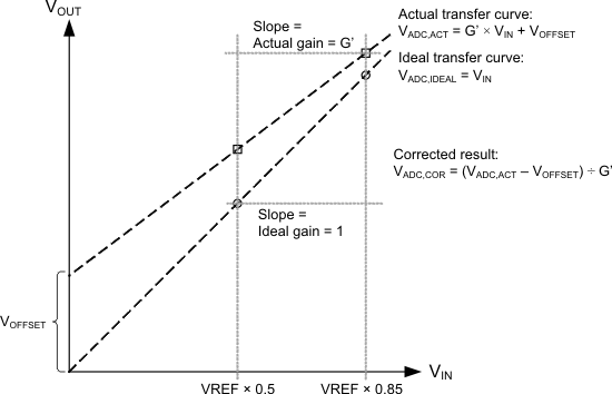
For applications where such ADC characterization is not provided or is not practical, the BQ76925 device provides a means for in-situ calibration of the Host ADC through setting of the VCOUT_SEL bits in the CELL_CTL register two scaled versions of the reference voltage, 0.5 × VREF and 0.85 × VREF, can be selected for output on the VCOUT pin for measurement by the Host ADC. Measuring both scaled voltages enables the Host to do a two-point calibration of the ADC and compensate for the ADC offset and gain in all subsequent ADC measurement results as shown in Figure 10.
Note that the calibration accuracy will be limited by the tolerance of the scaled reference-voltage output so that use of this method may not be effective. For these cases, TI recommends to use a higher-accuracy source for the two-point calibration shown in Figure 10.
 Figure 10. Host ADC Calibration Using VREF