SLUU406A February 2010 – January 2022 CSD16322Q5 , CSD16410Q5A , TPS40303 , TPS40304 , TPS40305
- Trademarks
- 1Description
- 2TPS40305EVM-488 Electrical Performance Specifications
- 3TPS40305EVM-488 Schematic
-
4Connector and Test Point Descriptions
- 4.1 Enable Jumper (JP2)
- 4.2 Frequency Spread Spectrum – FSS Jumper (JP1)
- 4.3
Test Point Descriptions
- 4.3.1 Input Voltage Monitoring (TP1 and TP2)
- 4.3.2 Output Voltage Monitoring (TP3 and TP4)
- 4.3.3 Loop Response Testing (TP5, TP6, TP7, TP8, and R3)
- 4.3.4 Error Amplifier Voltage Monitoring (TP9, TP10, and TP11)
- 4.3.5 Switching Waveform Monitoring (TP12, TP13, TP14, and TP15)
- 4.3.6 Power-Good Voltage Monitoring (TP16 and TP18)
- 4.3.7 Enable and Soft-Start Voltage Monitoring (TP17 and TP18)
- 5Test Set Up
- 6TPS40305EVM-488 Test Data
- 7TPS40305EVM-488 Assembly Drawings and Layout
- 8TPS40305EVM-488 Bill of Materials
- 9Revision History
7 TPS40305EVM-488 Assembly Drawings and Layout
Figure 7-1 through Figure 7-6 show the design of the TPS40305EVM-488 printed circuit board. The EVM has been designed using a 4-layer, 2-oz. copper-clad circuit board 2.5-inch × 2.5-inch with all populated components on the top to allow the user to easily view, probe. and evaluate the TPS40305 control IC in a practical double-sided application. Moving components to both sides of the PCB or using additional internal layers can offer additional size reduction for space constrained systems.
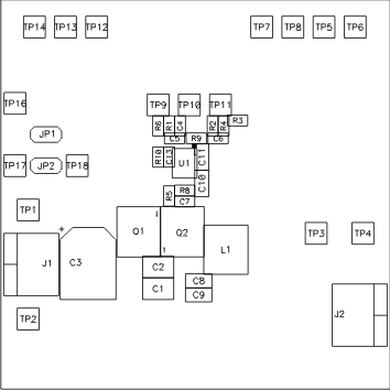 Figure 7-1 TPS40305EVM-488 Top Component Placement (Top View)
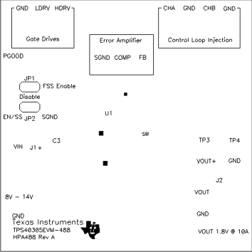 Figure 7-2 TPS40305EVM-488 Silk Screen (Top View)
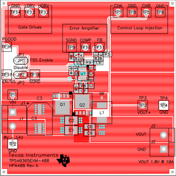 Figure 7-3 TPS40305EVM-488 Top Copper (Top View)
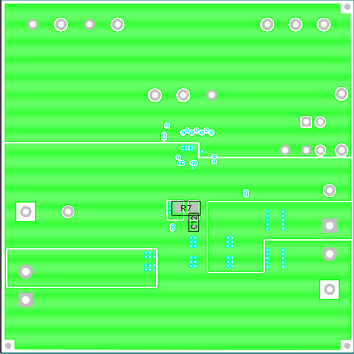 Figure 7-4 TPS40305EVM-488 Bottom Copper (Top View)
 Figure 7-5 TPS40305EVM-488 Internal 1 (X-Ray Top View)
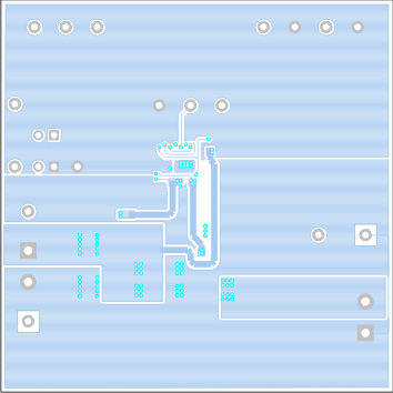 Figure 7-6 TPS40305EVM-488 Internal 2 (X-Ray Top View)