SLUU406A February 2010 – January 2022 CSD16322Q5 , CSD16410Q5A , TPS40303 , TPS40304 , TPS40305
- Trademarks
- 1Description
- 2TPS40305EVM-488 Electrical Performance Specifications
- 3TPS40305EVM-488 Schematic
-
4Connector and Test Point Descriptions
- 4.1 Enable Jumper (JP2)
- 4.2 Frequency Spread Spectrum – FSS Jumper (JP1)
- 4.3
Test Point Descriptions
- 4.3.1 Input Voltage Monitoring (TP1 and TP2)
- 4.3.2 Output Voltage Monitoring (TP3 and TP4)
- 4.3.3 Loop Response Testing (TP5, TP6, TP7, TP8, and R3)
- 4.3.4 Error Amplifier Voltage Monitoring (TP9, TP10, and TP11)
- 4.3.5 Switching Waveform Monitoring (TP12, TP13, TP14, and TP15)
- 4.3.6 Power-Good Voltage Monitoring (TP16 and TP18)
- 4.3.7 Enable and Soft-Start Voltage Monitoring (TP17 and TP18)
- 5Test Set Up
- 6TPS40305EVM-488 Test Data
- 7TPS40305EVM-488 Assembly Drawings and Layout
- 8TPS40305EVM-488 Bill of Materials
- 9Revision History
5.5 Control Loop Gain and Phase Measurement Procedure
- Follow steps 1 – 5 from Section 5.3 to set VIN and LOAD1 to desired operating condition.
- If JP1 is installed (FSS enabled), loop response data about the modulation frequency (30 kHz) can be affected.
- Connect a 1-kHz to 1-MHz isolation transformer to TP5 and TP7 as shown in Figure 5-3.
- Connect input signal amplitude measurement probe (channel A) to TP7 as shown in Figure 5-3
- Connect output signal amplitude measurement probe (channel B) to TP5 as shown in Figure 5-3.
- Connect ground lead of channel A and channel B to TP6 and TP8 as shown in Figure 5-3
- Inject 30-mV or less signal across R3 through an isolation transformer.
- Sweep frequency from 1 kHz to 1 MHz with 10-Hz or lower post filter.
- Control loop gain can be measured
by
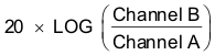 .
. - Control loop phase can be measured by the phase difference between channel A and channel B.
- Control to output response (power stage transfer function) can be measured by connecting channel A probe to TP10 (COMP) and channel B probe to TP5 (CHB).
- Output to control response (compensated error amplifier transfer function) can be measured by connecting channel A probe to TP7 (CHA) and channel B probe to TP10 (COMP).
- Follow steps 6 and 7 from Section 5.3 to power down.