SLUUB60B May 2015 – August 2021 TPS544B25 , TPS544C25
- Trademarks
- 1 Introduction
- 2 Description
- 3 EVM Electrical Performance Specifications
- 4 Schematic
- 5 Test Setup
- 6 EVM Configuration Using the Fusion GUI
- 7 Test Procedure
- 8 Performance Data and Typical Characteristic Curves
- 9 Fusion GUI
- 10EVM Assembly Drawing and PCB Layout
- 11List of Materials
- 12Revision History
10 EVM Assembly Drawing and PCB Layout
Figure 10-1 through Figure 10-6 show the design of the PWR-681EVM printed-circuit board (PCB).
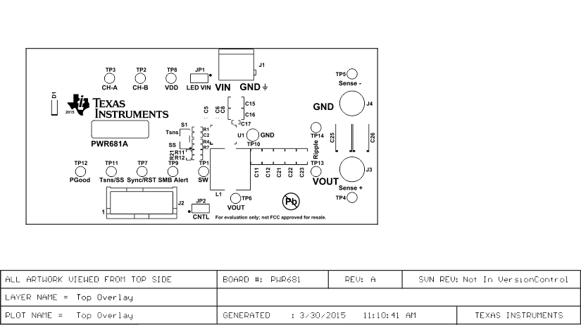 Figure 10-1 PWR-681EVM Top Layer Assembly Drawing (top view)
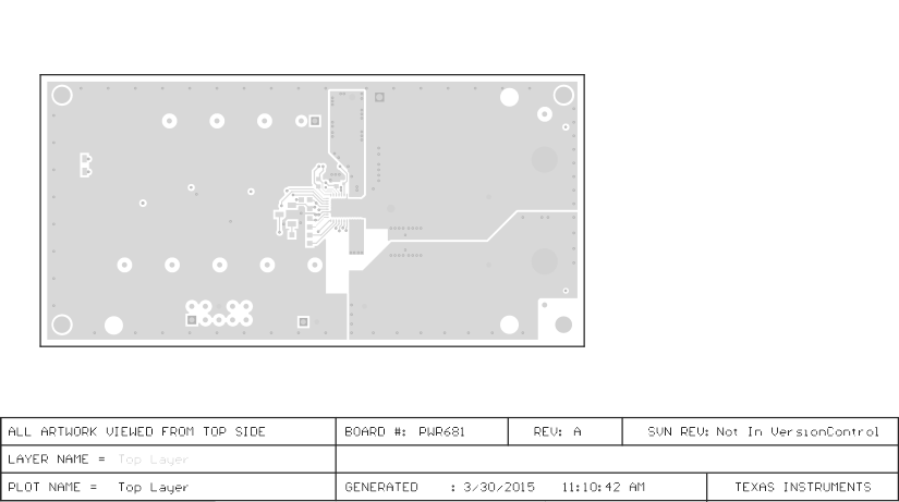 Figure 10-2 PWR-681EVM Top Layer (top view)
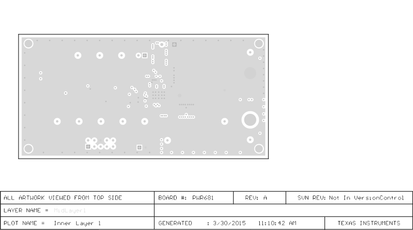 Figure 10-3 PWR-681EVM Layer 1 (top view)
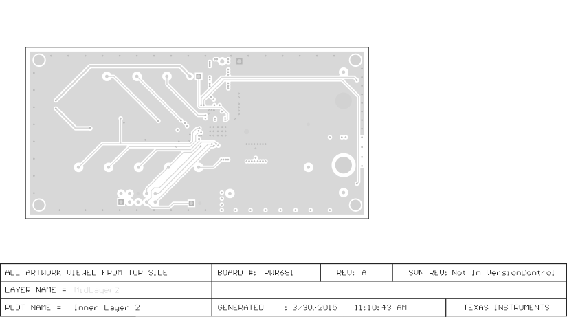 Figure 10-4 PWR-681EVM Layer 2 (top view)
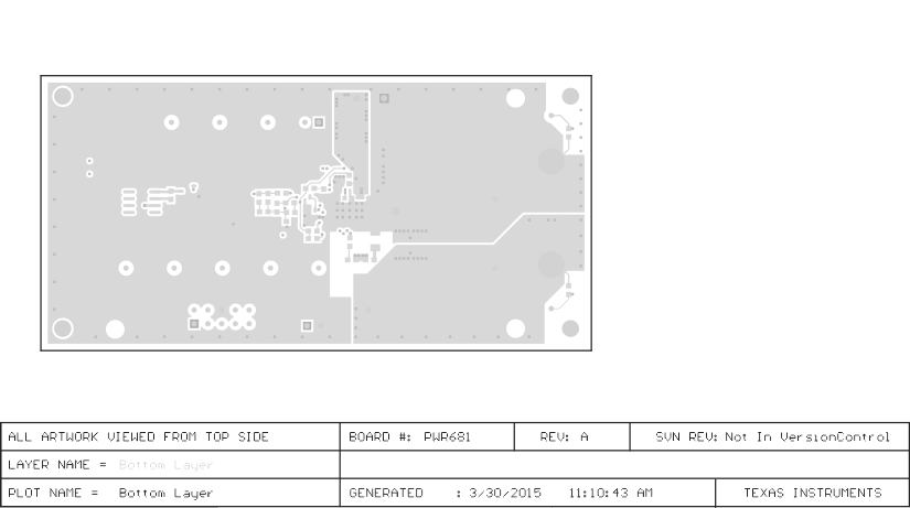 Figure 10-5 PWR-681EVM Bottom Layer (top view)
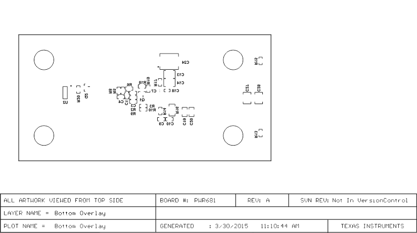 Figure 10-6 PWR-681EVM Bottom Layer Assembly Drawing (top view)