SLVA469D June 2013 – January 2023 TLV62130 , TLV62130A , TLV62150 , TLV62150A , TPS61175 , TPS61175-Q1 , TPS62130 , TPS62130A , TPS62131 , TPS62132 , TPS62133 , TPS62135 , TPS62136 , TPS62140 , TPS62140A , TPS62141 , TPS62142 , TPS62143 , TPS62150 , TPS62150A , TPS62151 , TPS62152 , TPS62153 , TPS62160 , TPS62161 , TPS62162 , TPS62163 , TPS62170 , TPS62171 , TPS62172 , TPS62173
1.2 Output Current Calculations
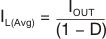
The average inductor current is also affected in this topology. In the buck configuration, the average inductor current is equal to the average output current because the inductor always supplies current to the load during both the on and off times of the control MOSFET. However, in the inverting buck-boost configuration, the load is supplied with current only from the output capacitor and is completely disconnected from the inductor during the on time of the control MOSFET. During the off time, the inductor connects to both the output capacitor and the load (see Figure 1-3). Knowing that the off time is (1 – D) of the switching period, Equation 1 can be used to calculate the average inductor current:
The operating duty cycle for an inverting buck-boost converter can be found with Equation 2:
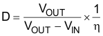
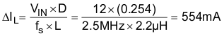
rather than VOUT/VIN for a buck converter. The efficiency term in Equation 2 adjusts the equations in this section for power conversion losses and yields a more accurate maximum output current result. The peak-to-peak inductor ripple current is given by Equation 3:

where:
- ΔIL (A): the peak-to-peak inductor ripple current
- D: duty cycle
- η: efficiency
- fS (MHz): switching frequency
- L (µH): inductor value
- VIN (V): the input voltage with respect to ground, not with respect to the device ground or VOUT
Equation 4 calculates the maximum inductor current:
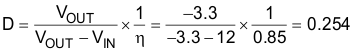
For example, for an output voltage of –3.3 V, 2.2-μH inductor, and input voltage of 12 V, the following calculations produce the maximum allowable output current that can be ensured based on the TPS62150 minimum current limit value of 1.4 A. The efficiency term is estimated at 85%.
Rearranging Equation 4 and setting IL(max) equal to the minimum value of ILIMF, as specified in the datasheet, gives:
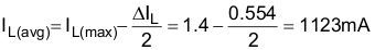
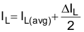
This result is then used in Equation 1 to calculate the maximum achievable output current:

Table 1-1 provides several examples of the calculated maximum output currents for different output voltages (–1.8 V, –3.3 V and –5 V) based on an inductor value and switching frequency of 2.2 µH and 2.5 MHz, respectively. Increasing the inductance and/or input voltage allows higher output currents in the inverting buck-boost configuration, while using the low frequency setting decreases the available output current. The maximum output currents for the TPS62150 in the inverting buck-boost topology are frequently lower than 1000 mA due to the fact that the average inductor current is higher than that of a typical buck. The output current for the same three output voltages and different input voltages is displayed in Figure 1-4.
| fs (MHz) | 2.5 | 2.5 | 2.5 |
| VOUT (V) | –5 | –3.3 | –1.8 |
| L (µH) | 2.2 | 2.2 | 2.2 |
| VIN (V) | 12 | 12 | 12 |
| IL(max) (A) | 1.4 | 1.4 | 1.4 |
| η | 0.85 | 0.85 | 0.85 |
| D | 0.346 | 0.254 | 0.153 |
| ∆IL (mA) | 755 | 554 | 335 |
| IL(avg) (mA) | 1023 | 1123 | 1233 |
| IOUT (mA) | 669 | 838 | 1043 |
 Figure 1-4 Maximum Output Current versus VIN