SLVA469D June 2013 – January 2023 TLV62130 , TLV62130A , TLV62150 , TLV62150A , TPS61175 , TPS61175-Q1 , TPS62130 , TPS62130A , TPS62131 , TPS62132 , TPS62133 , TPS62135 , TPS62136 , TPS62140 , TPS62140A , TPS62141 , TPS62142 , TPS62143 , TPS62150 , TPS62150A , TPS62151 , TPS62152 , TPS62153 , TPS62160 , TPS62161 , TPS62162 , TPS62163 , TPS62170 , TPS62171 , TPS62172 , TPS62173
4 Typical Performance
The reference design shown in Figure 4-1 was used to generate the typical characteristic graphs presented in this section and illustrated in Figure 4-2 through Figure 4-10.
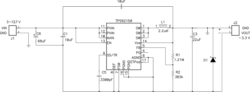 Figure 4-1 Schematic of the Tested Circuit
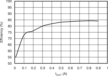 Figure 4-2 Efficiency vs Load Current with VIN = 12 V
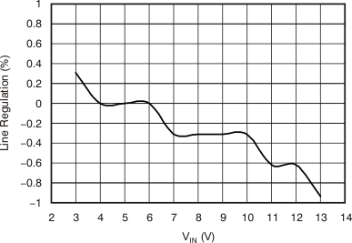 Figure 4-4 Line
Regulation at 500-mA Load
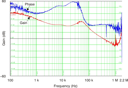 Figure 4-6 Bode
Plot at VIN = 12 V and 500-mA Load
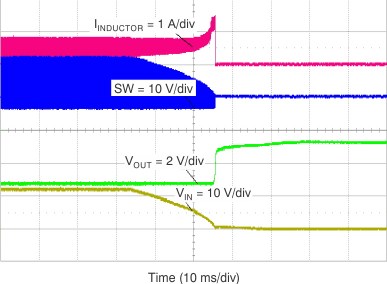 Figure 4-8 Shutdown on VIN at 500-mA Load
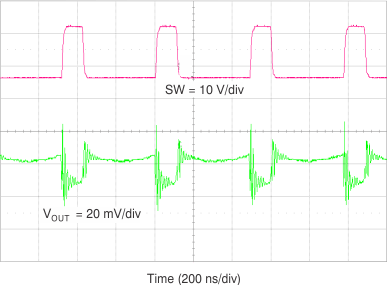 Figure 4-10 Output Voltage Ripple, VIN = 12 V and IOUT = 500
mA
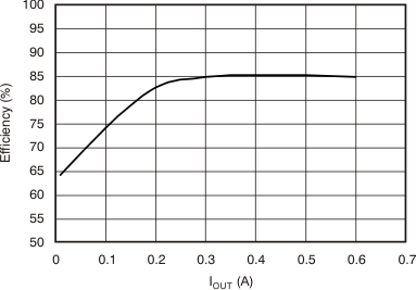 Figure 4-3 Efficiency vs Load Current with VIN = 5 V
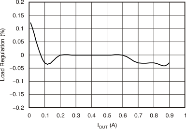 Figure 4-5 Load
Regulation at VIN = 12 V
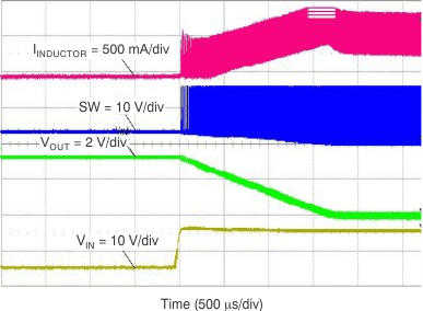 Figure 4-7 Startup on VIN at 160-mA Load
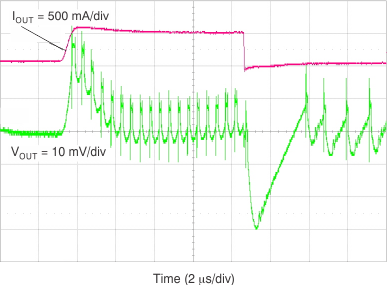 Figure 4-9 Load
Transient Response, 0 mA to 500 mA with VIN = 12V