SLVAE32B August 2018 – December 2023 TPS7H2201-SP
- 1
- Abstract
- Trademarks
- 1 Device Overview
- 2 Single-Event Effects
- 3 Test Device and Evaluation Board Information
- 4 Depth, Range, and LETEFF Calculation
- 5 Irradiation Facility and Setup
- 6 Test Setup and Procedures
- 7 Single-Event-Latchup (SEL), Single-Event-Burnout (SEB), and Single-Event-Gate-Rupture (SEGR)
- 8 Single Event Transient (SET)
- 9 Total Ionizing Dose From SEE Experiments
- 10Orbital Environment Estimations
- 11Confidence Interval Calculations
- 12Summary
- 13References
- 14Revision History
4 Depth, Range, and LETEFF Calculation
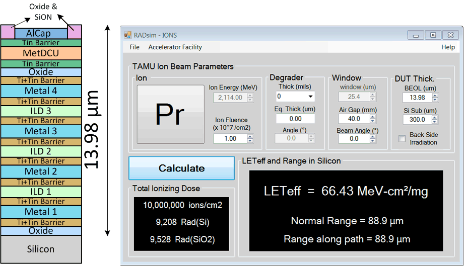
 Figure 4-1 Generalized Cross-Section (Left) of the LBC7
Technology BEOL Stack on the TPS7H2201-SP. GUI of RADsim Application
(Right)
Figure 4-1 Generalized Cross-Section (Left) of the LBC7
Technology BEOL Stack on the TPS7H2201-SP. GUI of RADsim Application
(Right)The TPS7H2201-SP is fabricated in the TI Linear BiCMOS 7, 250 nm process with a back-end-of-line (BEOL) stack consisting of four levels of aluminum. The total stack height from the surface of the passivation to the silicon surface is 13.98 µm based on nominal layer thickness as shown in Figure 4-1. Accounting for energy loss through the 1 mil thick Aramica ( Kevlar®) beam port window, the 40-mm air gap, and the BEOL stack over the TPS7H2201-SP, the effective LET (LETEFF) at the surface of the silicon substrate and the depth and ion range was determined with the custom RADsim-IONS application (developed at Texas Instruments and based on the latest SRIM2013 [9] models). Table 4-1 lists the results.
| Ion Type | Angle of Incidence (°) | Depth in Silicon (µm) | Range in Silicon (µm) | LETEFF (MeV·cm2 / mg) |
|---|---|---|---|---|
| Pr | 0 | 88.9 | 88.9 | 66.43 |
| Pr | 27.3 | 77.7 | 87.2 | 75 |