SLVAE49C April 2019 – April 2022 DRV8847 , DRV8873-Q1 , DRV8904-Q1 , DRV8906-Q1 , DRV8908-Q1 , DRV8910-Q1 , DRV8912-Q1
3.1 Circuit Operation and Detection
Figure 3-3 shows the circuit implementation of the active OLD in integrated drivers. The high-side FET of the OUT1 channel and low-side FET of the OUT2 are in the operating state. A reference voltage generator generates equivalent reference voltages for the OLD comparators' negative input terminals, while the positive terminals reflect the actual voltage in the FETs. As shown in Figure 3-3, the outputs of OL1_HS and OL2_LS are set to "1" when the output voltages (VOUT1_HS and VOUT2_LS) become greater than the reference voltage (VOL_REF) of the comparators,
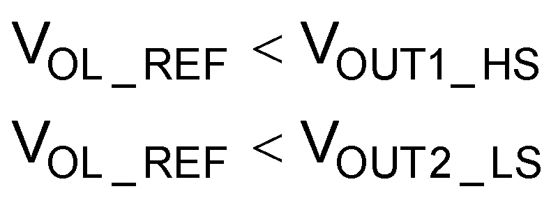
In this example, the reference-FET is any of the four FETs tied to the current reference sources (IOL_REF). The VOL_REF is determined by IOL_REF and the on-state resistance of the reference-FET (RDS(ON)_REF). Now, the VOUT1_HS and the VOUT2_LS are determined by the current and on-state resistances (RDS(ON)) through the FETs that drive the load. When an OLD event occurs, the current through the FETs must be greater than the OLD current threshold. For these equations, the current through the FETs is called IOL. Hence, by putting all of these parameters in Equation 14, the equation VOL_REF equation is modified to,

Hence, the IOLD can be calculated as,
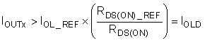
Equation 16 shows that the OLD depends on the on-state resistance ratio of the reference-FETs to the FETs driving the load.
Putting the values of on-state resistance ratio (450:1) and the reference generator pull-down current (20 µA), the OLD current threshold can be calculated as,
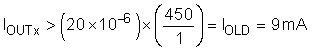
Hence, if current through the load is greater than 9 mA while OLD is active, an OLD event is registered.
 Figure 3-3 Active OLD Circuit in Brushed
DC Motor Integrated Drivers
Figure 3-3 Active OLD Circuit in Brushed
DC Motor Integrated DriversAs for the circuit implementation in DRV8873, DRV8873-Q1 and the DRV824x-Q1 devices, Figure 3-4 shows the circuit implementation of the active OLD of DRV8873/DRV8873-Q1. For the OL1_HS comparator, if the drain-to-source voltage across the high-side driving FET is less than the VOL_HS OLD threshold, OLD1_HS output is set to "1" and an OLD is detected. For the OL2_HS comparator, if the body diode voltage (VD) is less than the VOL_HS OLD threshold, OLD2_HS output is set to "1" and an OLD is detected. Due to the current re-circulation through the body diode (IOL), the body diode voltage (VD) depends on IOUTX for an OLD to occur.
There is a dependency on the operating conditions and on external circuitry, such as the output capacitors, that can cause an OLD to be reported even though the load is present. This case might occur during a direction change or for small load currents respectively small PWM duty cycles.
Figure 3-5 shows the circuit implementation for the active OLD of DRV824x-Q1. Device can detect an open load detection in the ACTIVE state during high-side recirculation. This includes high-side load connected directly to VM or through a high-side FET on the other half-bridge. During a PWM switching transition, the inductive load current re-circulates into VM through the HS body diode when the LS FET is turned OFF. The device looks for a voltage spike on OUTx above VM during the brief dead time, before the HS FET is turned ON. To observe the voltage spike, this load current needs to be higher than the pull down current (IPD_OLA) on the output asserted by the FET driver. Absence of this voltage spike for "3" consecutive re-circulation switching cycles indicates a loss of load inductance or increase in load resistance and is detected as an active open detection fault.
Finally, when using active OLD in gate drivers, capacitors must be placed between the load phase nodes and GND. These capacitor are required for BLDC motors and both bi-directional and unidirectional BDC motors at the phase nodes. If a solenoid load is connected, the capacitors are not required. Capacitors must be sized as:
 Figure 3-4 Circuit for Active OLD in a
DRV8873-Q1 and in a DRV8873 device
Figure 3-4 Circuit for Active OLD in a
DRV8873-Q1 and in a DRV8873 device Figure 3-6 Circuit for Active OLD in a
BLDC Gate Driver
Figure 3-6 Circuit for Active OLD in a
BLDC Gate Driver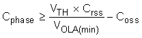
Where VTH is the threshold voltage of the FETs and VOLA(min) in the DRV8343-Q1 and DRV8340-Q1 is 150 mV. The values of the FET Crss and Coss should be used for 0 V VDS. Derating of Cphase must be considered when selecting the capacitance.