SLVAEX0 October 2020 TPS1H000-Q1 , TPS1H100-Q1 , TPS1H200A-Q1 , TPS1HA08-Q1 , TPS1HB16-Q1 , TPS1HB50-Q1 , TPS2HB16-Q1 , TPS2HB50-Q1 , TPS4H000-Q1 , TPS4H160-Q1
2.2.4 External Factor: Component Tolerances
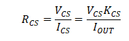
To use the CS pin, an external resistor is used by the device to convert the current from the current mirror to a voltage. This voltage is proportional to the load and can be used by the ADC to measure the current. Equation 1 shows the relationship between the resistor RCS, the current sense voltage VCS, the current sense current ICS, the current sense ratio KCS, and the output current IOUT.
The SNS pin requires a resistor that should be selected that allows for the largest load current that puts the voltage VSNS at about 90% of the ADC’s full scale value as to differentiate from a fault value on the SNS pin. Along with this requirement, the smallest load current must keep VSNS from falling below 1 LSB of the ADC. Table 2-7 and the following calculation show an example of the sense resistor calculation to ensure that the max load of 1.5A meets the 95% requirement and the minimum load of 0.2A stays above the 1LSB in a 4-bit ADC
| Load (A) | Sense Ratio | ISNS (mA) | RSNS (Ω) | VSNS (V) | % of 3.3V ADC |
|---|---|---|---|---|---|
| 1.5 | 1500 | 1 | 3.01k | 3.01 | 91% |
| 0.2 | 1500 | 0.133 | 3.01k | 0.401 | 12% |
As the 0.012 V/bit step size is smaller than the lowest sense voltage, a standard resistor closest to 3.01k Ω will be acceptable in this application.
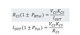
The tolerance of the external resistor impacts the accuracy of the current sense. With a device that works better as it gets closer to the rated operating current, the smart high side switches will be impacted by the tolerance of the current sense resistor as shown where the tolerance of the resistance is represented as a decimal PRTol. The effect of the resistor Equation 3 tolerance can be seen in where RCS is the current sense resistor, PRTol is the resistor tolerance, VCS is the current sense voltage, KCS is the current sense ratio, and IOUT is the output current.
Devices that have a SNS or CS pin will already have a specified deviation for the current sense accuracy such as the TPS1HB08-Q1 with a ± 5% accuracy when the current output is 10A. For best results, a 1% tolerance or less should be used to ensure minimum error.