SLVAEZ2 September 2020 – MONTH TPSM41625
5 Improving Stability by Decreasing the Voltage Reference and Adding a Feedforward Capacitor
The use of a feedforward capacitor (CFF) to increase loop bandwidth and phase margin is well documented in other application reports (2). One consideration when using a feedforward capacitor is that the maximum possible phase boost is limited by the ratio of the reference voltage to the output voltage. The maximum possible phase boost for a given reference voltage (VREF) and output voltage (VOUT) can be calculated using Equation 1 or determined using Figure 5-1.
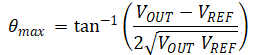

Figure 5-1 Maximum phase boost with feedforward capacitor
The results shown in this report thus far have been with a reference voltage of 1.1 V. For a 1.8-V output with a 1.1-V reference, the ratio is 1.1 V / 1.8 V = 0.61 V/V and the maximum possible phase boost with a CFF capacitor is only 14°. Recall that the 300-μF output capacitor design switching at 500 kHz has a phase margin of 24.5°, thus, the CFF capacitor alone cannot provide sufficient phase boost to increase the phase margin above 45°. Furthermore, the maximum theoretical phase boost cannot be realized directly as phase margin improvement because CFF boosts the phase and the gain such that the crossover frequency also increases to where there is more phase lag in the loop.
To increase the amount of CFF phase boost, it is necessary to lower the reference voltage. The TPSM41625 has 10 selectable internal reference voltage options ranging from 0.6 V to 1.1 V. The reference voltage is programmed with a resistor RVSEL connected from VSEL pin to AGND. By using the 0.6-V reference (VREF / VOUT = 0.33 V/V), the maximum phase boost possible with CFF increases to 30°. The changes required to switch from the 1.1-V to the 0.6-V reference voltage are shown in Figure 5-2. The RVSEL resistor of 187 kΩ is replaced with a short to AGND. The RADJ resistor is increased from 634 Ω to 2 kΩ to keep the output voltage set at 1.8 V.

Figure 5-2 Changes to lower reference voltage and add feedforward capacitor
Switching to the 0.6-V reference has other impacts on stability in addition to increasing the maximum CFF phase boost. Lowering the reference voltage decreases the divider gain and lowers the entire gain curve, lowering the crossover frequency and increasing the phase and gain margin. Figure 5-3 shows the Bode plot with the original 1.1-V reference and 0.6-V reference. By switching to the 0.6-V reference, the crossover frequency has reduced from 105 kHz to 79 kHz, phase margin has increased from 24.5° to 29°, and gain margin has increased from 12.5 dB to 16.7 dB.
")
Figure 5-3 Bode plot with lower reference voltage and feedforward capacitor (12-V input, 1.8-V output, 20-A load)
Figure 5-3 also shows the measured Bode plot for 0.6-V reference with a 1.2-nF CFF capacitor which shows the final stable design with a crossover frequency of 87 kHz, phase margin of 52.5°, and gain margin of 16 dB. These are all meeting the recommended criteria for a stable design. The final schematic with all modifications is shown in Figure 5-4.

Figure 5-4 Original and Optimized 12-V input, 1.8-V output, 25-A, 500-kHz design with 3 x 100 μF of ceramic output capacitance
Figure 5-5 and Figure 5-6 show the transient response for a 0 to 5-A step at 10 A/μs with the 0.6-V reference without and with the 1.2-nF feedforward capacitor, respectively. The ringing is clearly reduced with the addition of the feedforward capacitor, and the transient undershoot and overshoot remain within ±3% of the 1.8-V output. Figure 5-7 shows a larger step of 0 to 10 A at 10 A/μs, showing a transient deviation of about ±5%.
There is a tradeoff in using the lower reference voltage, however: the output voltage accuracy is reduced. Assuming ideal resistors and ignoring all other error sources such as resistor tolerance, the ±0.5% reference accuracy will reflect as a ±1.5% (±0.5% × 1.8 V / 0.6 V ) accuracy at the output for the 0.6-V reference, compared to ±0.81% (±0.5% × 1.8 V / 1.1 V) accuracy for the 1.1-V reference. This may be an acceptable tradeoff for stabilizing a minimum ceramic output capacitor design and maintaining 500-kHz operation at high efficiency.

Figure 5-5 Load transient 0 to 5 A at 10 A/μs without CFF

Figure 5-7 Load transient 0 to 10 A at 10 A/μs with 1.2-nF CFF

Figure 5-6 Load transient 0 to 5 A at 10 A/μs with 1.2-nF CFF