SLVAEZ2 September 2020 – MONTH TPSM41625
4 Effect of Switching Frequency on Loop Response
The switching frequency of the TPSM41625 is adjustable from 300 kHz to 1 MHz and is programmed by a resistor connected between the RT pin and AGND. The TPSM41625 can also be synchronized to an external clock. Frequency synchronization is useful for applications that require multiple power rails to be synchronized to the same switching frequency to avoid beat frequency problems on the common input power line.
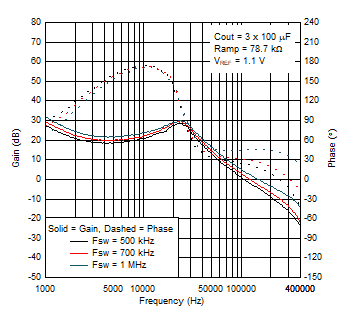
Figure 4-1 shows the loop response of the 300-μF output capacitor design with the 78.7-kΩ ramp resistor for switching frequencies of 500 kHz, 700 kHz, and 1 MHz. Higher switching frequencies improve the stability of the module as the Fsw/2 pole moves higher resulting in higher phase maintained near the crossover. The loop response for 1 MHz has a phase margin of 46.2°, indicating a stable design, and its crossover frequency of 146 kHz is below 1/5 of the switching frequency and is acceptable.
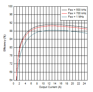
Switching at higher frequencies has a tradeoff of higher switching losses and lower efficiency. The efficiency at different switching frequencies is shown in Figure 4-2. At a switching frequency of 500 kHz, the efficiency is 91% peak and 89.5% at full 25-A load. At 1 MHz, the efficiency is 88.5% peak and 86.9% at full 25-A load, which translates to 1.6 W of higher power dissipation at full load when operating at 1 MHz versus at 500 kHz.
Therefore, while switching at 1 MHz provides a more stable design, the lower efficiency and higher power dissipation may be undesirable. Moving to higher switching frequency may also not be allowed if the application requires lower switching frequency to minimize switching harmonic content from falling into certain frequency bands, and, as previously mentioned, if the application requires the module to be synchronized with other power rails that are switching at a given frequency. Different approaches to improve phase margin must be used to maintain the high efficiency and operate at the original 500-kHz switching frequency of the design.

Figure 4-1 Bode plot for different switching frequency (12-V input, 1.8-V output)

Figure 4-2 Efficiency for different switching frequency (12-V input, 1.8-V output)