SLVSFG1A January   2021  – May 2021 TPS2116

PRODUCTION DATA  

  1. Features
  2. Applications
  3. Description
  4. Revision History
  5. Pin Configuration and Functions
  6. Specifications
    1. 6.1 Absolute Maximum Ratings
    2. 6.2 ESD Ratings
    3. 6.3 Recommended Operating Conditions
    4. 6.4 Thermal Information
    5. 6.5 Electrical Characteristics
    6. 6.6 Switching Characteristics
    7. 6.7 Timing Diagrams
    8. 6.8 Typical Characteristics
  7. Detailed Description
    1. 7.1 Overview
    2. 7.2 Functional Block Diagram
    3. 7.3 Feature Description
      1. 7.3.1 Truth Table
      2. 7.3.2 Soft Start
      3. 7.3.3 Status Indication
      4. 7.3.4 Reverse Current Blocking
    4. 7.4 VINx Collapse Rate
    5. 7.5 Output Voltage Drop
    6. 7.6 Device Functional Modes
      1. 7.6.1 Priority/Manual Mode
        1. 7.6.1.1 Priority Switching
        2. 7.6.1.2 Manual Switching
  8. Application and Implementation
    1. 8.1 Application Information
    2. 8.2 Typical Application
      1. 8.2.1 Design Requirements
      2. 8.2.2 Detailed Design Procedure
      3. 8.2.3 Application Curves
  9. Power Supply Recommendations
  10. 10Layout
    1. 10.1 Layout Guidelines
    2. 10.2 Layout Example
  11. 11Device and Documentation Support
    1. 11.1 Documentation Support
      1. 11.1.1 Related Documentation
    2. 11.2 Receiving Notification of Documentation Updates
    3. 11.3 Trademarks
    4. 11.4 Electrostatic Discharge Caution
    5. 11.5 Glossary
  12. 12Mechanical, Packaging, and Orderable Information

Reverse Current Blocking

The TPS2116 initiates reverse current blocking (RCB) when the VOUT voltage is externally biased and exceeds the input voltage supply being used. Once the output voltage is higher than the input voltage by 42mV (VRCB,R), the device will shut off. During this state, the leakage into VOUT and out of VIN is defined by IREV. Once the voltage difference between the output and input lowers to 17mV (VRCB,F), the channel will turn back on.
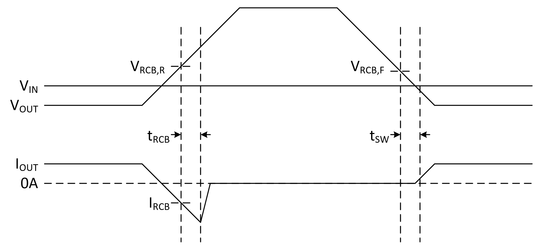
GUID-20210511-CA0I-CS6B-S0TC-H1ZPPS3P9CSX-low.jpgFigure 7-1 Reverse Current Blocking Behavior

If RCB is expected to occur, it is recommended to clamp the output or use a high output capacitance (about 100µF). This will prevent voltage spikes from damaging the device due to output inductance.