SLVUBT0A June 2020 – January 2021
3.4 Configuration Headers
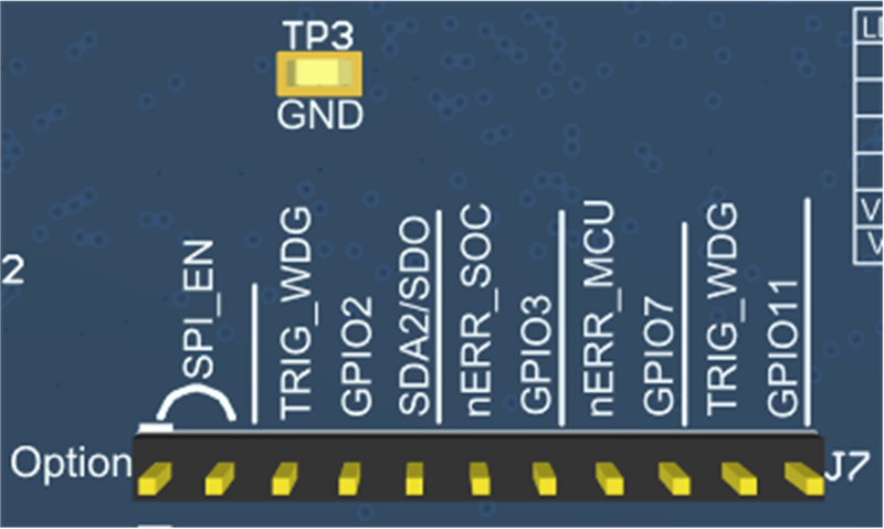
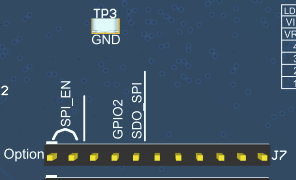
There are six headers available to configure the EVM function. Headers J26 and J37 configure the backup power supply and master and slave mode of operation respectively. J45 is connected to J37, which can pull the nPWRON/ENABLE pin of the PMIC to a logic high or low. Header J7, as shown in the silk screen picture in Figure 3-1 and Figure 3-2, is used to configure the EVM to match the feature setting written to the device configuration registers. J30 is used to select the PMIC IO voltage, either 1.8 V or 3.3 V. The sixth header is a portion of J15, which allows VSYS to be powered from the USB connection and the configuration of GPIO1.
 Figure 3-1 TPS6594EVM Header J7
 Figure 3-2 TPS6593EVM Header J7
| Option Pins | Configuration | Description | |
|---|---|---|---|
| SPI_EN | Open (Default) | I2C Mode. The signal path for I2C communication between the MCU and the PMIC is enabled. | |
| Closed | SPI mode. The signal path for SPI communication between the MCU and the PMIC is enabled. | ||
| TRIG_WDG, GPIO2, SDA2/SDO | Open | GPIO mode. GPIO2 from PMIC is connected to PM7 of the MCU through a level translator. | |
| TRIG_WDG, GPIO2: Closed | Trigger Watchdog mode. GPIO2 of the PMIC should be in the Alternative function to support the watchdog trigger input signal. GPIO2 from the PMIC is connected to the MCU output and TRIG_WDG. | ||
| GPIO2,SDA2/SDO: Closed (Default) | I2C Mode (J7 VIO_IN, I2C/SPI: Open) | Q&A Watchdog mode. GPIO2 of the PMIC should be in the Alternative function to support the Q&A Watchdog and the I2C mode is selected. This setting is done in conjunction with J15, GPIO1,SCL2/CS: Closed. | |
| SPI mode (J7 VIO_IN, I2C/SPI: Closed) | SPI mode, Chip Select. GPIO2 of the PMIC should be in the Alternative function to support SPI communication. This setting is done in conjunction with J15, GPIO1, SCL2/CS: Closed. | ||
| ERR_SoC, GPIO3 | Open (Default) | GPIO mode. GPIO3 of the PMIC is connected to PP5 of the through a level translator. | |
| Closed | SoC Error Count Down mode. GPIO3 of the PMIC should be in the Alternative function to support the system error count down from the SoC. GPIO is connected to alternative MCU output, nERR_SoC. | ||
| ERR_MCU, GPIO7 | Open (Default) | GPIO mode. GPIO7 of the PMIC is connected to POH of the through a level translator. | |
| Closed | MCU Error Count Down mode. GPIO7 of the PMIC should be in the Alternative function to support the system error count down from the MCU. GPIO7 is connected to MCU output PK5, nERR_MCU. | ||
| TRIG_WDG, GPIO11 | Open (Default) | GPIO mode. GPIO11 from PMIC is connected to PP4 of the MCU through a level translator. | |
| Closed | Trigger Watchdog mode. GPIO11 of the PMIC should be in the Alternative function to support the watchdog trigger input signal. GPIO11 from the PMIC is connected to the MCU output PK4, TRIG_WDG. | ||
| Configuration | Description |
|---|---|
| Open | VBACKUP is not connected. |
| Pin1, Pin2: Closed (Default) | VCCA is connected to the PMIC Battery Backup and VBACKUP. |
| Pin2, Pin3: Closed | Cell C3 is connected to the PMIC Battery Backup and VBACKUP.(1) |
| Configuration | Description1 |
|---|---|
| Open | Not Allowed, 1.8 V or 3.3 V must be selected. |
| VIO Select, 3.3 V: Closed (Default) | VIO_IN is 3.3 V. |
| VIO Select, 1.8 V: Closed | VIO_IN is 1.8 V. |
- In addition to J7 and J26, the lower portion of J15 is also used for the selection of VSYS and GPIO1.
| Configuration | Description1 | |
|---|---|---|
| V3V3, VSYS: Closed (Default) | 3.3 V from U13 is connected to VSYS (VCCA). U13 is supplied with the 5 V from the USB connection (VBUS) through J47. VBUS is not intended to support heavy load conditions of greater than 3 W. This is the default state of the EVM | |
| VSYS, V5V0, and V3V3: Open | VSYS, VBUS, and USB_3V3 are isolated. VSYS should be powered from J6. | |
| VSYS, V5V0: Closed | 5 V from U14 is connected to VSYS (VCCA). U14 is supplied with the 5 V from the USB connection (VBUS) through J47. VBUS is not intended to support heavy load conditions of greater than 3 W. | |
| SCL2/CS, GPIO1: Open | GPIO mode. GPIO1 of the PMIC is connected to IO1 of the MCU. | |
| SCL2/CS, GPIO1: Closed (Default) | I2C mode (J7 SPI_EN: Open) | Q&A Watchdog mode. GPIO1 of the PMIC should be in the Alternative function to support the Q&A Watchdog and the I2C mode selected. This setting is done in conjunction with J7, GPIO2, SDA2/SDO: Closed |
| SPI mode (J7 SPI_EN: Closed) | SPI mode, Chip Select. GPIO1 of the PMIC should be in the Alternative function to support SPI communication. This setting is done in conjunction with J7, GPIO2, SDA2/SDO: Closed | |
- The PMIC device can be configured for a power good level of 3.3 V or 5.0 V for the VCCA pin. Align the V3V3/VSYS/VBUS jumper with the PMIC configuration. The default PMIC configuration is 3.3 V.