SLVUDN8 March   2026


  1.   1
  2.   Description
  3.   Features
  4.   Applications
  5.   5
  6. 1Evaluation Module Overview
    1. 1.1 Introduction
    2. 1.2 Kit Contents
    3. 1.3 Specification
    4. 1.4 Device Information
  7. 2Hardware
    1. 2.1 Connector, Test Point, and Jumper Descriptions
      1. 2.1.1 Connector and Test Point Descriptions
      2. 2.1.2 Jumper Configuration
        1. 2.1.2.1 JP1 and JP2 (I2C Interface Enable)
        2. 2.1.2.2 JP3 (Boost Enable)
        3. 2.1.2.3 JP4 (Status or DRV Pin)
        4. 2.1.2.4 JP5 (TS Pin)
        5. 2.1.2.5 JP6 (Charger Enable)
        6. 2.1.2.6 JP7 (LDO Enable)
    2. 2.2 Test Procedure
      1. 2.2.1 Verifying Boost Function
      2. 2.2.2 Verifying Charger Function
      3. 2.2.3 Verifying SOH Function
  8. 3Software
    1. 3.1 Software User Interface
      1. 3.1.1 Install USB2ANY Explorer
      2. 3.1.2 GUI Installation
      3. 3.1.3 Interface Hardware Setup
      4. 3.1.4 User Configuration Screen
      5. 3.1.5 Status and Fault Indications Screen
      6. 3.1.6 Register Map Screen
    2. 3.2 Modification
  9. 4Hardware Design Files
    1. 4.1 Schematic
    2. 4.2 PCB Layout
    3. 4.3 Bill of Materials
  10. 5Additional Information
    1. 5.1 Trademarks
  11. 6Revision History

PCB Layout

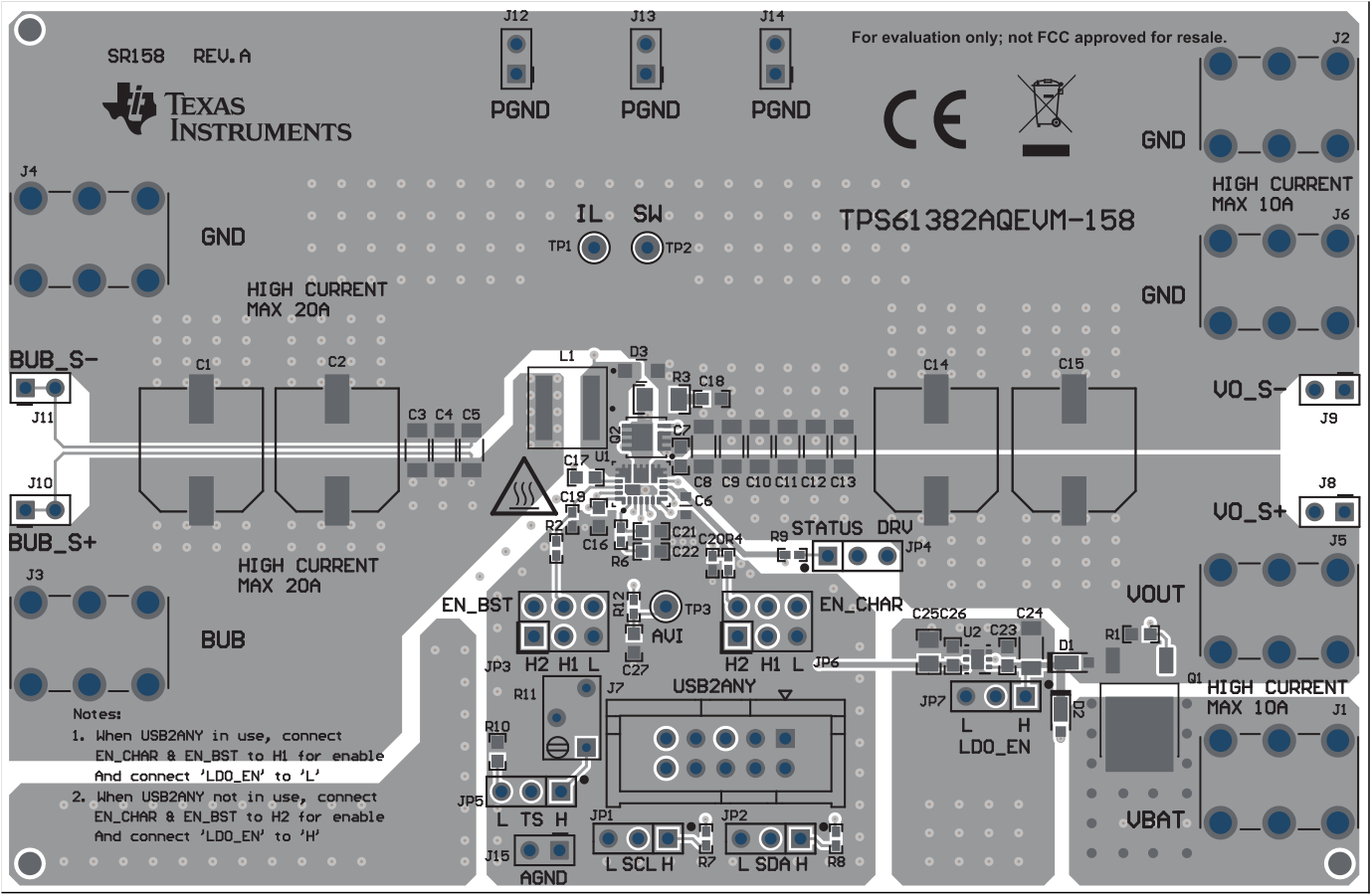
TPS61382AQEVM-158 TPS61382AQEVM-158 Top-Side LayoutFigure 4-2 TPS61382AQEVM-158 Top-Side Layout
TPS61382AQEVM-158 TPS61382AQEVM-158 Inner Layer1Figure 4-3 TPS61382AQEVM-158 Inner Layer1
TPS61382AQEVM-158 TPS61382AQEVM-158 Inner Layer2Figure 4-4 TPS61382AQEVM-158 Inner Layer2
TPS61382AQEVM-158 TPS61382AQEVM-158 Bottom-Side LayoutFigure 4-5 TPS61382AQEVM-158 Bottom-Side Layout