SNOSDE6C December 2022 – August 2025 LM74900-Q1 , LM74910-Q1 , LM74910H-Q1
PRODUCTION DATA
- 1
- 1 Features
- 2 Applications
- 3 Description
- 4 Device Comparison Table
- 5 Pin Configuration and Functions
- 6 Specifications
- 7 Parameter Measurement Information
-
8 Detailed Description
- 8.1 Overview
- 8.2 Functional Block Diagram
- 8.3 Feature Description
- 8.4 Device Functional Modes
-
9 Applications and Implementation
- 9.1 Application Information
- 9.2
Typical 12V Reverse Battery Protection Application
- 9.2.1 Design Requirements for 12V Battery Protection
- 9.2.2 Automotive Reverse Battery Protection
- 9.2.3
Detailed Design Procedure
- 9.2.3.1 Design Considerations
- 9.2.3.2 Charge Pump Capacitance VCAP
- 9.2.3.3 Input and Output Capacitance
- 9.2.3.4 Hold-Up Capacitance
- 9.2.3.5 Selection of Current Sense Resistor, RSNS
- 9.2.3.6 Selection of Scaling Resistor (RSET) and Short-Circuit Protection Setting Resistor (RSCP)
- 9.2.3.7 Overcurrent Limit (ILIM), Circuit Breaker Timer (TMR), and Current Monitoring Output (IMON) Selection
- 9.2.3.8 Overvoltage Protection and Battery Monitor
- 9.2.4 MOSFET Selection: Blocking MOSFET Q1
- 9.2.5 MOSFET Selection: Hot-Swap MOSFET Q2
- 9.2.6 TVS Selection
- 9.2.7 Application Curves
- 9.3 Addressing Automotive Input Reverse Battery Protection Topologies With LM749x0-Q1
- 9.4 Power Supply Recommendations
- 9.5 Layout
- 10Device and Documentation Support
- 11Revision History
- 12Mechanical, Packaging, and Orderable Information
6.7 Typical Characteristics
 Figure 6-1 Operating Quiescent Current vs Supply Voltage
 Figure 6-3 SLEEP Mode Current vs Supply Voltage
A.
Figure 6-5 Charge Pump Current vs Supply Voltage at CAP – VS ≥ 6 V (LM74910-Q1)
A.
Figure 6-7 Charge Pump V-I Characteristics at VS ≥ 12 V (LM74910-Q1)
A.
Figure 6-9 HGATE Drive Voltage vs Supply Voltage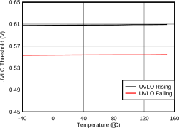
A.
Figure 6-11 UVLO Thresholds vs Temperature
A.
Figure 6-13 Charge Pump UVLO Threshold vs Temperature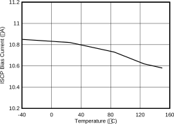 Figure 6-15 ISCP Bias Current vs Temperature
 Figure 6-17 VS POR Threshold vs Temperature
 Figure 6-19 DGATE Turn On Delay During Forward Conduction
 Figure 6-21 HGATE Turn OFF Delay During SCP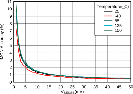
A.
Figure 6-23 LM74910H-Q1, IMON Accuracy (%) vs VSENSE (mV) Figure 6-2 Shutdown Current vs Supply Voltage
A.
Figure 6-4 Charge Pump Current vs Supply Voltage at CAP – VS ≥ 6 V (LM74900-Q1)
A.
Figure 6-6 Charge Pump V-I Characteristics at VS ≥ 12 V (LM74900-Q1)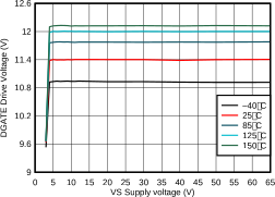
A.
Figure 6-8 DGATE Drive Voltage vs Supply Voltage
A.
Figure 6-10 ANODE Leakage Current vs Reverse ANODE Voltage
A.
Figure 6-12 OVP Thresholds vs Temperature Figure 6-14 ISCP to CS– Threshold vs Temperature
A.
Figure 6-16 VA POR Threshold vs Temperature Figure 6-18 DGATE Turn OFF Delay
 Figure 6-20 HGATE Turn OFF Delay During OV
A.
Figure 6-22 Current Monitor Output vs Sense Voltage (RIMON = 5kΩ, RSET = 50Ω)