SNOU176B October 2020 – March 2022
PRODUCTION DATA
- Trademarks
- 1 General TI High Voltage Evaluation User Safety Guidelines
- 2 Introduction
- 3 LMG342XEVM-04X Schematic
- 4 Mother Board Schematic
- 5 Recommended Footprint
- 6 Test Equipment
- 7 Test Procedure When Paired With LMG342X-BB-EVM
- 8 Test Procedure When Paired With LMG34XX-BB-EVM
- 9 Bill of Materials
- 10Revision History
2.1.4 Heat Sink
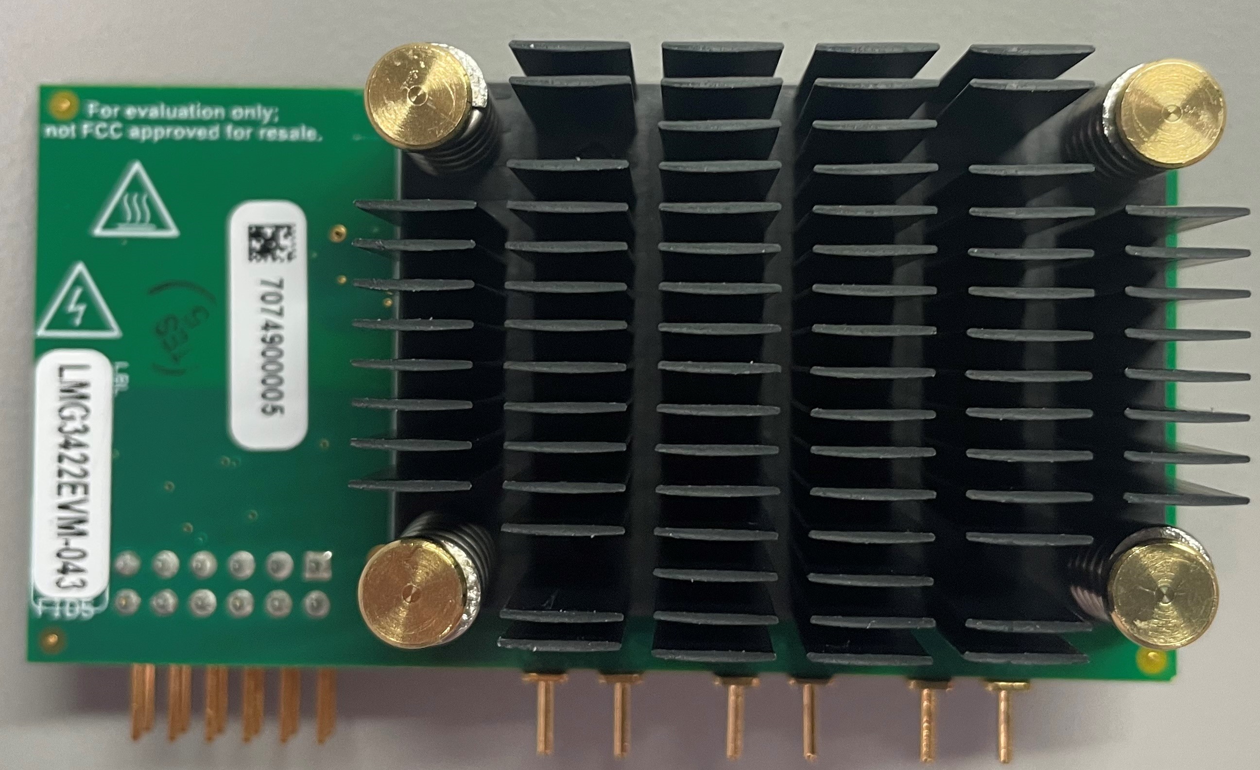
The heat sink is installed to help with heat dissipation of the LMG342XR0X0. Exposed copper pads are attached to the die attach pad (DAP) on the high-side and low-side devices to provide a low thermal impedance point for the heat sink. The two copper pads have a high-voltage potential difference between them, therefore an electrically isolated thermal interface material (TIM) is required.
For optimal thermal dissipation and board level reliability, recommendation for thermal via pattern and solder paste example are provided in the LMG342xR030 600-V 30-mΩ GaN FET With Integrated Driver, Protection, and Temperature Reporting data sheet. Pin numbers 1, 16, 17 and 54 are NC (no connection) which are used to anchor QFN package to PCB. These pins must be soldered to PCB landing pads which have to be non-solder mask defined pads and must not be physically connected to any other metal on the PCB. Internally, pins 1 and 16 are connected to DRAIN and pins 17 and 54 are connected to SOURCE/GND and THERMAL PAD. All pads must be NSMD for mechanical performance, refer to the device datasheet for trace connection recommendations to the pads. Filling the thermal pad with thermal vias is recommended for thermal performance. Vias must be filled and planarized.
In this daughter card design, 'S05MZZ12-A' heatsink and 'GR80A-0H-50GY' (thermal conductivity of 8 W/m·K and thickness of 0.5 mm), thermal interface material has been used. More details on thermal performance and comparison between different TIM are shown in Thermal Performance of QFN 12x12 Package for 600-V GaN Power Stage application note.
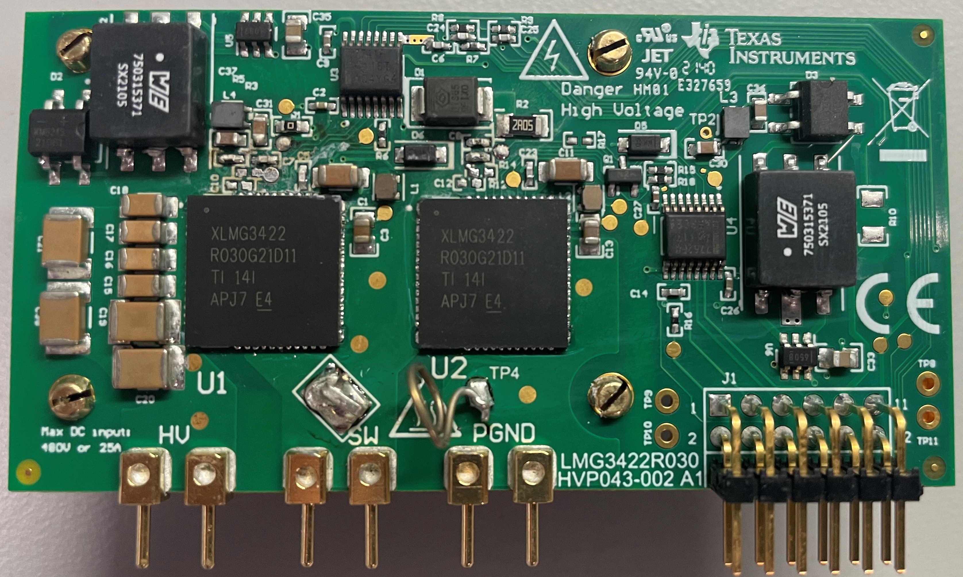
 Figure 2-2 Front Side View of the EVM
 Figure 2-3 Back Side View of the EVM