SNOU176B October 2020 – March 2022
PRODUCTION DATA
- Trademarks
- 1 General TI High Voltage Evaluation User Safety Guidelines
- 2 Introduction
- 3 LMG342XEVM-04X Schematic
- 4 Mother Board Schematic
- 5 Recommended Footprint
- 6 Test Equipment
- 7 Test Procedure When Paired With LMG342X-BB-EVM
- 8 Test Procedure When Paired With LMG34XX-BB-EVM
- 9 Bill of Materials
- 10Revision History
2.1 LMG342XEVM-04X Daughter Card
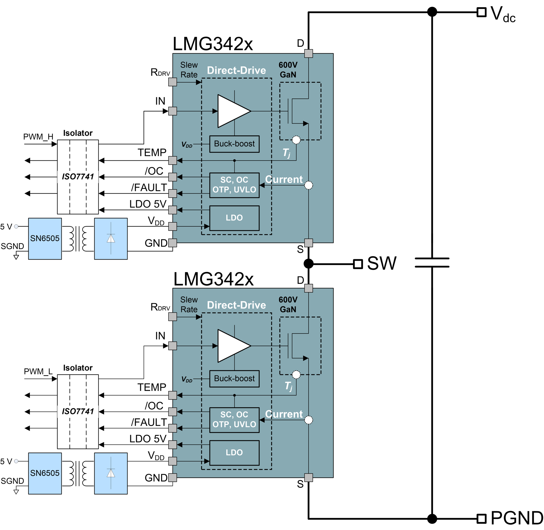
The LMG342XEVM-04X has two LMG342XR0X0 GaN FETs in a half-bridge configuration. All the bias and level shifting components are included, which allows low-side referenced signals to control both FETs. High-frequency decoupling capacitors are included on the power stage in an optimized layout to minimize parasitic inductance and reduce voltage overshoot.
The layout of the board is critical to device's performance and functionality. TI prefers a four-layer or higher layer count board to reduce the parasitic inductance of the layout to achieve suitable performance. Layout guidelines are provided in the LMG342xR030 600-V 30-mΩ GaN FET With Integrated Driver, Protection, and Temperature Reporting data sheet to optimize the solder-joint reliability, power loop inductance, signal to ground connection, switched-node capacitance and thermal heat dissipation.
| EVM NAME | FEATURED GaN FET WITH INTEGRATED DRIVER AND PROTECTION |
|---|---|
| LMG3422EVM-041 | LMG3422R050 |
| LMG3422EVM-043 | LMG3422R030 |
| LMG3425EVM-041 | LMG3422R050 |
| LMG3425EVM-043 | LMG3425R030 |
There are 12 logic pins on the LMG342XEVM-04X.
| PIN | PIN DESIGNATION | DESCRIPTION |
|---|---|---|
| LS PWM | 1 | Logic gate signal input for low-side LMG342XR0X0. Compatible with both 3.3-V and 5-V logic. Referenced to AGND. |
| HS TEMP | 2 | PWM TEMP output for high-side LMG342XR0X0. Referenced to AGND. |
| LS Fault | 3 | FAULT output signal for low-side LMG342XR0X0. Referenced to AGND. |
| HS OC | 4 | OC output signal for high-side LMG342XR0X0. Referenced to AGND. |
| LS OC | 5 | OC output signal for low-side LMG342XR0X0. Referenced to AGND. |
| HS Fault | 6 | FAULT output signal for high-side LMG342XR0X0. Referenced to AGND. |
| LS Temp | 7 | PWM TEMP output for low-side LMG342XR0X0 . Referenced to AGND. |
| HS PWM | 8 | Logic gate signal input for high-side LMG342XR0X0. Compatible with both 3.3-V and 5-V logic. Referenced to AGND. |
| 12V | 9 | Auxiliary power input for when the LMG342XEVM-04X is configured in bootstrap mode. Pin is not used when configured in isolated power mode. |
| 5V | 10 | Auxiliary power input for the LMG342XEVM-04X. Used to power logic isolators. Used as input bias power of LMG342XR0X0 devices when configured in isolated power mode. |
| AGND | 11,12 | Logic and bias power ground return pin. Functionally isolated from PGND. |
There are six power pins on the LMG342XEVM-04X.
| PIN | DESCRIPTION |
|---|---|
| SW | Switch node of the half-bridge configuration |
| HV | Input DC voltage of the half-bridge configuration |
| PGND | Power ground of the half-bridge configuration. Functionally isolated from AGND. |
 Figure 2-1 LMG342XEVM-04X Block Diagram
High-voltage levels are present on the evaluation module whenever it is energized. Take proper precautions when working with the EVM.