SNVA941A June 2020 – November 2022 LM5156 , LM5156-Q1 , LM51561 , LM51561-Q1 , LM51561H , LM51561H-Q1 , LM5156H , LM5156H-Q1
- How to Design a Boost Converter Using the LM5156
- 1LM5156 Design Example
- 2Example Application
-
3Calculations and Component Selection
- 3.1 Switching Frequency
- 3.2 Inductor Calculation
- 3.3 Current Sense Resistor Calculation
- 3.4 Inductor Selection
- 3.5 Diode Selection
- 3.6 MOSFET Selection
- 3.7 Output Capacitor Selection
- 3.8 Input Capacitor Selection
- 3.9 UVLO Resistor Selection
- 3.10 Soft-Start Capacitor Selection.
- 3.11 Feedback Resistor Selection
- 3.12 Control Loop Compensation
- 3.13 Efficiency Estimation
- 4Component Selection Summary
- 5Small-Signal Frequency Analysis
- 6Revision History
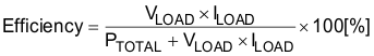
3.13 Efficiency Estimation
The total loss of the boost converter (PTOTAL) can be expressed as the sum of the losses in the device (PIC), MOSFET power losses (PQ), diode power losses (PD), inductor power losses (PL), and the loss in the sense resistor (PRS).

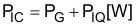
PIC can be separated into gate driving loss (PG) and the losses caused by quiescent current (PIQ).
Each power loss is approximately calculated as follows:
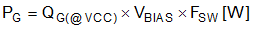
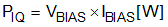
For IBIAS values in each mode, see the LM5156 data sheet.
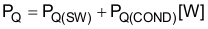
PQ can be separated into switching loss (PQ(SW)) and conduction loss (PQ(COND)).
Each power loss is approximately calculated as follows:

tR and tF are the rise and fall times of the low-side N-channel MOSFET device. ISUPPLY is the input supply current of the boost converter.
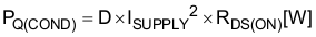
RDS(on) is the on-resistance of the MOSFET and is specified in the MOSFET data sheet. Consider the RDS(on) increase due to self-heating.
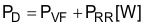
PD can be separated into diode conduction loss (PVF) and reverse recovery loss (PRR).
Each power loss is approximately calculated as follows:
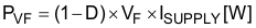

QRR is the reverse recovery charge of the diode and is specified in the diode data sheet. Reverse recovery characteristics of the diode strongly affect efficiency, especially when the load voltage is high.
PL is the sum of DCR loss (PDCR) and AC core loss (PAC). DCR is the DC resistance of inductor which is mentioned in the inductor data sheet.
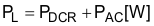
Each power loss is approximately calculated as follows:


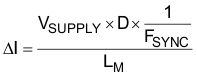
∆I is the peak-to-peak inductor current ripple. K, α, and β are core dependent factors which can be provided by the inductor manufacturer.
PRS is calculated as follows:

Efficiency of the power converter can be estimated as follows: