SNVAA25A January 2022 – July 2022 DP83TD510E , ESDS302 , LM5155 , LM66100 , MSP430FR2476 , TL431LI , TLV3012
3.2 Coupling and Decoupling Network (CDN)
The PD must decouple power from the power and data path on the SPE link in a safe manner while allowing the data to pass through to the 10BASE-T1L PHY transparently and with no impact on the signal integrity. In addition, the IEEE 802.3cg standard specifies that the PD may receive power in two modes with power input pins swapped.
Table 3-1 details the PD pinout.
| Contact | Mode A | Mode B |
|---|---|---|
| 1 | PI+ | PI– |
| 2 | PI– | PI+ |
To protect the PD and implement it a manner insensitive to the polarity of the power supply, the PD includes a rectifier bridge. The Schottky diodes were carefully chosen to give a low-voltage drop across the rectifier.
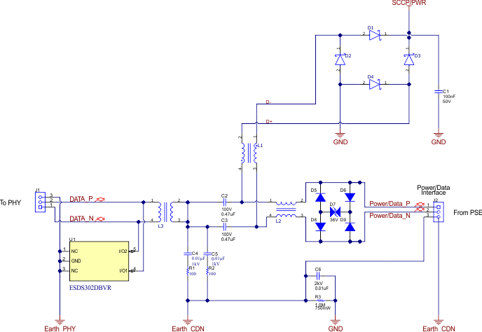
The mode of operation of the CDN is as follows: Power and data come in on a SPE cable. Following the protection circuit (diodes D5 through D9), a common-mode choke (CMC) L2 suppresses common-mode noise and capacitors C2 and C3 provide the necessary damping. The common-mode noise must be filtered out without affecting the integrity of the differential signal. For this, a CMC with large common-mode impedance and small differential mode impedance in the 10-kHz range was selected.
The transformer L3 then provides isolation and the ESD diode is included for ESD protection. The choice of the transformer is dependent on the application, desired isolation rating as well as good performance in the appropriate frequency range. The inductance of the transformer has a direct impact on the droop.
From the CMC, a low DCR differential mode inductor (DMI) L1 allows DC current to pass to the rectifier (diodes D1 through D4). The rectifier ensures correct polarity to the PD regardless of cable orientation. The saturation current of the DMI must be sufficient for the desired power class (for class 12, this is at minimum 632 mA) and the DCR should be as low as possible to maximize efficiency and minimize the voltage drop, especially when designing for a 1-km cable reach. The inductance of the DMI has to be high enough to not cause too much damping of the data.
Figure 3-2 shows the PD coupling and decoupling network.

Figure 3-2 PD Coupling and Decoupling Network
Additional points of note are the termination between CDN ground and PD ground to minimize EMI (R3 and C6) as well as the common mode termination (C4, C5, R1, and R2).