SNVAA25A January 2022 – July 2022 DP83TD510E , ESDS302 , LM5155 , LM66100 , MSP430FR2476 , TL431LI , TLV3012
3.4 SCCP Communication
Serial Communication Classification Protocol (SCCP) is the bidirectional, single-wire serial communication protocol specified by the IEEE 802.3bu standard (and amended in IEEE 802.3cg) for negotiating power transfer requirements between the PSE and PD before the PSE applies power to the link. SCCP is current-sinking and wired-OR. During SCCP, the PSE acts as a controller, controlling the PD target device. The VID current source on the PSE is used as the pullup and the SCCP line is driven by pulling it low with discrete MOSFETs. The implementation of SCCP is optional if detection is implemented correctly on the PD and PSE. When classification is skipped in the system, this can be referred to as Fast Start-up Mode.
See the IEEE 802.3bu and 802.3cg standards for timing definitions. This document summarizes how to implement compliant SCCP communication on the PD. SCCP communication starts with a reset pulse from the PSE, which is followed by a presence pulse from the PD. In SCCP, every transaction starts with the falling edge from the PSE, which can read “1” or ”0” depending on the low logic time – so called “Write 1 time slot” and “Write 0 time slot”. For reading, the PD pulls the line low after a certain specified time. The PD can only transmit data to the PSE when the PSE issues read time slots. When the read time slot is started by the controller, the PD then transmits a “1” or ”0” by leaving the line high or driving it low.
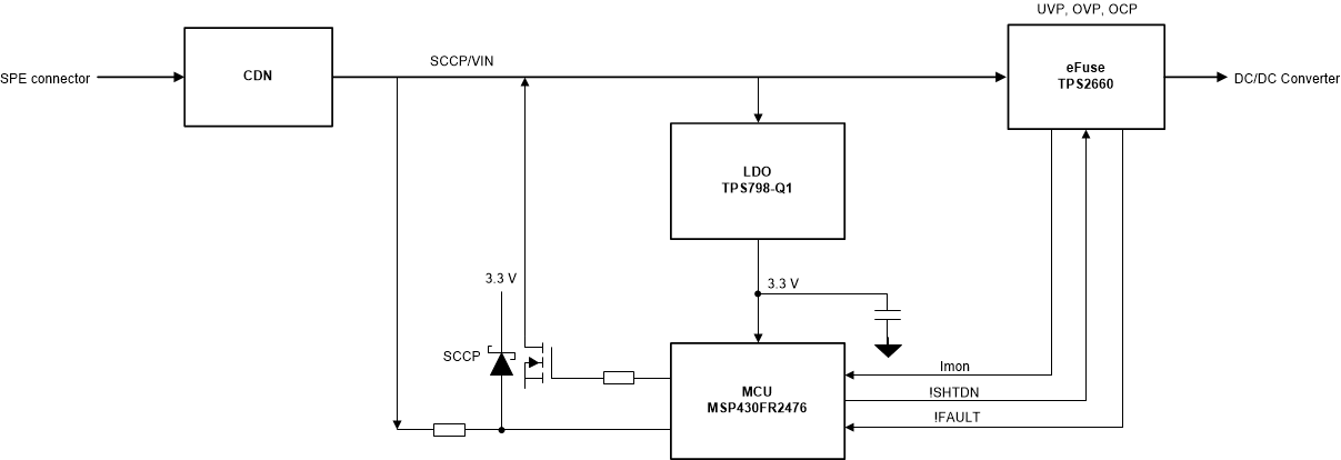
Due to the simplicity of the protocol and the relatively slow speed of 333 bps, one of the simplest SCCP implementations is by using only GPIO pins on the microcontroller and a clamping diode to limit the voltage at the pin when the line is high (24 V once the PSE applies power to the link).
Figure 3-5 shows the PD SCCP system blocks.

Figure 3-5 PD SCCP System Blocks
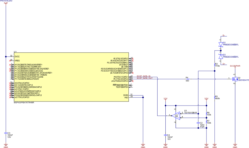
However, this approach can be improved by including a comparator as a buffer or driver on the data-in pin (U3 TLV7031). This ensures that the voltage rise and fall times are within specifications and the voltage into the GPIO pins does not exceed the supply voltage.
Figure 3-6 illustrates the PD simplified final SCCP circuit.

Figure 3-6 PD Simplified Final SCCP Circuit
It is important to note that during the reset pulse, the SCCP line gets pulled low for up to 11 ms. This line supplies the LDO, which in turn supplies the microcontroller in the PD with 3.3 V. As such, there must be enough energy stored in the output capacitor of the LDO to supply the MCU for the duration of the reset pulse. A 10-µF capacitor was found to be reliable on the PD board.
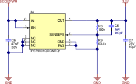
It is also a concern that the current will flow from the output capacitor into the output pin of the LDO during the reset pulse and all communication. To protect against this, an LDO with reverse current blocking at the output can be used. This PD design takes advantage of the TPS798-Q1 automotive 50-mA LDO with reverse-current protection. An ideal diode controller such as the LM66100 can be used as an alternative when using an LDO without reverse-current protection.
Figure 3-7 shows the PD LDO circuit.

Figure 3-7 PD LDO Circuit
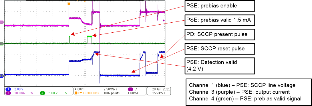
The oscilloscope screenshots in Figure 3-8 and Figure 3-9 show the start-up waveforms as seen on the PSE side. At first, the PSE supplies the PD with prebias voltage of 3.3 V so that the PD can operate in its low-power mode. The PSE tests the link with a detection current pulse and detects a valid voltage signature in the range of 4.05 V to 4.55 V. This is followed by a reset pulse initiated by the PSE, during which the PD microcontroller must remain functional, which then initiates SCCP communication.

Figure 3-8 PSE Start-up Behavior
SCCP communication takes place as previously outlined, during which the PSE and PD negotiate the power class. Following SCCP communication, the PSE applies power to the link.

Figure 3-9 PSE Start-up With SCCP