SNVSB66A July 2018 – October 2021 TPS3431
PRODUCTION DATA
- 1 Features
- 2 Applications
- 3 Description
- 4 Revision History
- 5 Pin Configuration and Functions
- 6 Specifications
- 7 Detailed Description
- 8 Application and Implementation
- 9 Power Supply Recommendations
- 10Layout
- 11Device and Documentation Support
- 12Mechanical, Packaging, and Orderable Information
5 Pin Configuration and Functions

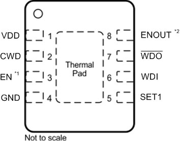
EN can also be left floating and is internally pulled-up to VDD
ENOUT can also be left floating or tied to
WDO
Figure 5-1 DRB Package:
TPS34313-mm × 3-mm VSON-8
Top View
Table 5-1 Pin Functions
| PIN | I/O | DESCRIPTION | |
|---|---|---|---|
| NAME | NO. | ||
| VDD | 1 | I | Supply voltage pin. For noisy systems, connecting a 0.1-μF bypass capacitor is recommended. |
| CWD | 2 | I | Programmable watchdog timeout input. The
watchdog timeout is set by connecting a capacitor between this pin and
ground. Connecting via a 10-kΩ resistor to VDD or leaving
unconnected further enables the selection of the preset watchdog
timeouts; see the CWD Functionality section. TheTPS3431 determines the watchdog timeout using Equation 1 |
| EN | 3 | I | Enable input pin. This pin is internally pulled up to VDD and must be logic high or left floating. When EN goes logic low, ENOUT goes logic low and WDI is ignored and WDO remains logic high. When EN goes logic high, ENOUT goes high (asserts) after the watchdog reset delay time (tRST). This pin can also be driven with an external push-button, transistor, or microcontroller. |
| GND | 4 | — | Ground pin |
| SET1 | 5 | I | Logic input. Grounding the SET1 pin disables the watchdog timer. SET1 and CWD select the watchdog timeouts; see the SET1 section. |
| WDI | 6 | I | Watchdog input. A falling
edge must occur at WDI before the timeout (tWD) expires. When the watchdog is not in use, the SET1 pin can be used to disable the watchdog. WDI is ignored when WDO is low (asserted) and when the watchdog is disabled. If the watchdog is disabled, WDI cannot be left unconnected and must be driven to either VDD or GND. |
| WDO | 7 | O | Watchdog open-drain active-low output. Connect WDO with a 1-kΩ to 100-kΩ resistor to the correct pull-up voltage rail (VPU). WDO goes low (asserts) when a watchdog timeout occurs. When a watchdog timeout occurs, WDO goes low (asserts) for the watchdog reset delay time (tRST). When EN goes low, WDO is in a high-impedance state and will be pulled to logic high. |
| ENOUT | 8 | O | Enable open-drain active-high output. Connect ENOUT with a 1-kΩ to 100-kΩ resistor to the correct pull-up voltage rail (VPU). When EN goes logic high, ENOUT goes high impedance and pulls logic high (asserts) due to the external pull-up resistor after the watchdog reset delay time (tRST). When EN is forced logic low, ENOUT goes low after 200 ns and remains logic low as long as EN is logic low. |
| Thermal pad | — | Connect the thermal pad to a large-area ground plane. The thermal pad is internally connected to GND. | |