SNVU663A June   2019  – May 2021 LP87524-Q1 , LP87524B-Q1 , LP87524J-Q1 , LP87524P-Q1


  1.   Trademarks
  2. 1Introduction
  3. 2Setup
    1. 2.1 SCL/SDA Pins
    2. 2.2 NRST Pin
    3. 2.3 ENx (GPIOx) Pins
    4. 2.4 nINT
  4. 3Configuration
    1. 3.1 Default OTP Configurations
      1. 3.1.1 LP87524B-Q1 OTP Configuration
        1. 3.1.1.1 Startup and Shutdown Sequence
      2. 3.1.2 LP87524J-Q1 OTP Configuration
        1. 3.1.2.1 Startup and Shutdown Sequence
      3. 3.1.3 LP87524P-Q1 OTP Configuration
        1. 3.1.3.1 Startup and Shutdown Sequence
  5. 4References
  6. 5Revision History

Startup and Shutdown Sequence

Figure 3-3 shows default startup and shutdown sequence programmed to OTP, in this case with EN1 signal. Refer to the datasheet for a full description of all registers and their settings.
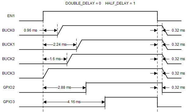
GUID-F69106CD-9769-4D43-B81C-FABCBAB1D53E-low.gifFigure 3-3 LP87524P-Q1 Startup and Shutdown Sequence Timing Diagram