SPRUIT8D February 2020 – February 2021 AWR2243
- Trademarks
- 1Getting Started
- 2Hardware
- 3Design Files and Software Tools
- 4Design Revision History
- 5Mechanical Mounting of PCB
- 6PCB Storage and Handling Recommendations
- 7Regulatory Information
- 8Revision History
2.4.1 20-Pin BoosterPack™ Connectors
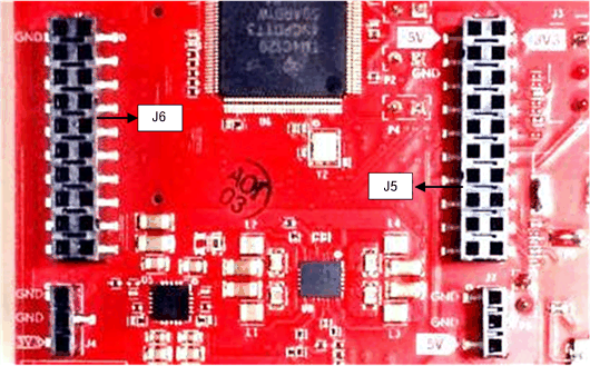
The BoosterPack has the standard LaunchPad connectors (J5 and J6) which enable the BoosterPack to be directly connected to all TI MCU LaunchPads (see Table 2-1). While connecting the BoosterPack to other LaunchPads, ensure the pin 1 orientation is correct by matching the 3V3 and 5-V signal marking on the boards (see Figure 2-6).
 Figure 2-6 20-Pin BoosterPack™ Connectors (J5 and J6)
Table 2-1 and Table 2-2 provide the connector-pin information.
Table 2-1 20-Pin Connector Definition (J6)
| Pin Number | Description | Pin Number | Description |
|---|---|---|---|
| 1 | NERROUT | 2 | GND |
| 3 | NERRIN | 4 | NC |
| 5 | MCUCLK OUT | 6 | SPI_CS |
| 7 | NC | 8 | GPIO1 |
| 9 | MSS LOGGER | 10 | nRESET |
| 11 | WARMRST | 12 | SPI_MOSI |
| 13 | BSS LOGGER | 14 | SPI_MISO |
| 15 | SOP2 | 16 | HOSTINT |
| 17 | SOP1 | 18 | GPIO2 |
| 19 | SOP0 | 20 | NC |
Table 2-2 20-Pin Connector Definition (J5)
| Pin Number | Description | Pin Number | Description |
|---|---|---|---|
| 1 | 3V3 | 2 | 5 V |
| 3 | NC | 4 | GND |
| 5 | RS232TX (Tx from IWR device) | 6 | ANA1 |
| 7 | RS232RX (Rx into IWR device) | 8 | ANA2 |
| 9 | SYNC_IN | 10 | ANA3 |
| 11 | NC | 12 | ANA4 |
| 13 | SPI_CLK | 14 | PGOOD (onboard VIO) |
| 15 | GPIO0 | 16 | PMIC Enable |
| 17 | SCL | 18 | SYNC_OUT |
| 19 | SDA | 20 | PMIC CLK OUT |
- PGOOD – This signal indicates the state of the onboard VIO supply for the AWR device coming from the onboard PMIC. A high on the PGOOD signal (3.3 V) indicates that the supply is stable. Because the IOs are not failsafe, the MCU must ensure that it does not drive any IO signals to the AWR device before this IO supply is stable. Otherwise, there could be leakage current into the IOs.
- PMIC Enable – This signal goes onboard PMIC enable. The MCU can use this signal to completely shut down the PMIC and AWR device to save power. The power up of the PMIC takes approximately 5 ms once the Enable signal is released.
Note:
To enable this feature, the R102 resister must be populated on the EVM.