SSZTBU1 December 2015 LMK03328 , LMK61E2 , LMK6C
High-performance clock oscillators and clock-generator integrated circuits (ICs) are pervasive in virtually all of today’s systems. Field-programmable gate arrays (FPGAs) find their place in a large variety of end equipment, owing to their functional flexibility and lower cost compared to a custom digital application-specific IC (ASIC). As a result, it is fairly common in a large variety of applications to find a high-performance oscillator or clock-generator IC providing the reference clock to an FPGA.
Depending on the end application, the external reference clock to an FPGA can come from fixed-frequency oscillators or serially programmable oscillators/clock-generator ICs.
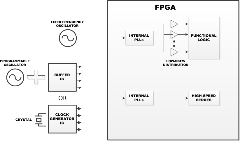
Fixed-frequency oscillators typically drive internal phase-locked loops (PLLs) in an FPGA (Figure 1). The internal PLLs provide clock multiplication and low-skew clock distribution to the various functional blocks within the FPGA (control plane clock).
The serializer/deserializer (SERDES) transceivers in complex FPGA implementations typically require an external reference clock with low integrated root-mean-square (RMS) jitter to minimize transceiver bit errors. Multirate transceivers require clocks of various frequencies. These needs are commonly addressed by electrically erasable programmable read-only memory (EEPROM)/I2C programmable oscillators and buffers, or high-performance multiple-output fractional-N PLL clock generators (Figure 1).
 Figure 1 Reference Clocks for
FPGAs
Figure 1 Reference Clocks for
FPGAsAn external serially programmable reference oscillator can also function as a digitally controlled oscillator (DCO) in certain FPGA applications (Figure 2). In such applications, the digital phase detector, digital loop filter and dividers/counters are implemented in the FPGA. The digital loop filter control word from the FPGA can be written into the programmable oscillator registers through the serial peripheral interface SPI/I2C interface. The oscillator adjusts its output frequency based on this loop filter control word. The frequency adjustment required in these applications is typically in parts per million (≤ ± 50 ppm from nominal) to track the recovered clock.
 Figure 2 Digital Controlled
Oscillator
Figure 2 Digital Controlled
OscillatorLet’s highlight some key guidelines for selecting an optimal reference-clocking solution for your FPGA-based design.
Flexibility
FPGA-based applications can optimize their power and throughput by selecting an optimal reference-clock rate. The ability to quickly change the FPGA reference clock during the prototype and validation phases of the design cycle enables system designers to help analyze timing margins and make the necessary logic updates to improve overall system performance/stability and reduce time to market. SERDES transceivers in complex FPGA implementations can potentially benefit from clock-rate optimization as well. Clock generators and high-performance oscillators with a serial programming interface, integrated EEPROM and hooks for output frequency margining provide the high level of flexibility required to streamline the overall product development cycle and optimize performance of the end system.
Availability
Custom frequency oscillators are often hard to procure and have long lead times. When time to market is critical to the success of the product, it is important to plan ahead and select the right clocking devices early in the design cycle, with the knowledge that system architectures can and probably will change over time. Factory lead times for custom fixed-frequency oscillators need to be short. The alternative is to select programmable oscillators and clock generators with integrated EEPROMs that allow multiple writes in your design.
Performance
Current FPGA-based transceivers are required to support high-speed data communication links (40/100 Gigabit Ethernet, optical transport networks (OTN), 3G – serial digital interface (3G-SDI) and Peripheral Component Interconnect Express (PCIe). The performance of the reference clock to these SERDES blocks within the FPGA becomes critical to minimize bit errors. Selecting a reference clock that has ultra-low integrated phase jitter ensures low bit-error rates for data transported over these high-speed links. It is wise to future-proof your system by selecting a reference clock that can provide significant timing margins for today’s systems.
Power-supply noise rejection (PSNR) is another critical specification for reference clocks in FPGA-based systems. Switching power supplies (DC/DC converters) and high edge rates of logic-level transitions within the FPGA can introduce significant noise in these systems. Identifying the noise sources and minimizing their impact by adding external passive filter networks can get expensive and time-consuming. Off-the-shelf oscillators are notorious for poor PSNR. Select oscillators and clock generators have integrated low-dropout regulators (LDOs) on their supply pins, which makes them more resilient to external power-supply noise.
Reliability
Standard quartz crystal-based oscillators (non-temperature-compensated) are susceptible to frequency perturbations over temperature (activity dips). These activity dips can potentially result in intermittent system failures. You can screen crystals exhibiting these frequency perturbations over temperature during production. Ask your quartz-based crystal-oscillator vendor if they test their device for frequency perturbation over temperature.
Crystals are also susceptible to startup issues due to contamination (internal and external factors). Consider replacing multiple crystals and/or oscillators in your system using a clock-generator IC.
Texas Instruments has a healthy portfolio of flexible and high-performance clock generators, clock jitter cleaners, radio frequency (RF) PLLs/synthesizers, clock buffers and oscillators to meet the stringent needs of your FPGA-based applications. When it comes to FPGA-based designs, my favorite clock generator and programmable oscillator are the LMK03328 and LMK61E2, respectively.
Additional Resources
- To learn more about frequency margining, download these TI application reports:
- Ease evaluation for the LMK03328 and the LMK61E2 with evaluation modules.
- Watch a video to learn how to “Optimize system performance and design time with the LMK03328 ultra-low-jitter clock generator.”
- Watch a video to learn how to “improve system performance with TI’s new customizable, ultra-low-jitter oscillators.”
- Find out more about TI’s clocks and timing portfolio.
- Read other technical articles about clocks and timing design challenges.