SWRU493C July   2024  – January 2025 CC2564C


  1.   1
  2.   Trademarks
  3. 1Introduction to the CC256xCQFN-EM Board
    1. 1.1 Key Features
    2. 1.2 QFN EM Board Applications
  4. 2Module Description
  5. 3Module Detailed Description
    1. 3.1 Pin Description
      1. 3.1.1 Board Jumpers
        1. 3.1.1.1 Measuring Current Consumption
      2. 3.1.2 Antenna and U.FL Selector
      3. 3.1.3 RF Connectors
      4. 3.1.4 Debug Header
      5. 3.1.5 COM Connector
    2. 3.2 Clock Inputs
  6. 4Module Dimensions
  7. 5Tools and Software
    1. 5.1 TI's Bluetooth Software Solution
    2. 5.2 Evaluation Platforms
    3. 5.3 Bluetooth Hardware Evaluation Tool
  8. 6Certification
  9. 7Life Support Policy
  10. 8References
  11. 9Revision History

Module Detailed Description

The reference files including schematics, layout, and BOM for the CC256xCQFN-EM board can be found in the CC256XCQFN-EM Design Files.

Figure 3-1 shows a block diagram depicting the I/Os of the QFN board that are required for interfacing to the host controller. These I/Os can be interfaced to the host controller through either the COM connector or the RF1 and RF2 sockets.
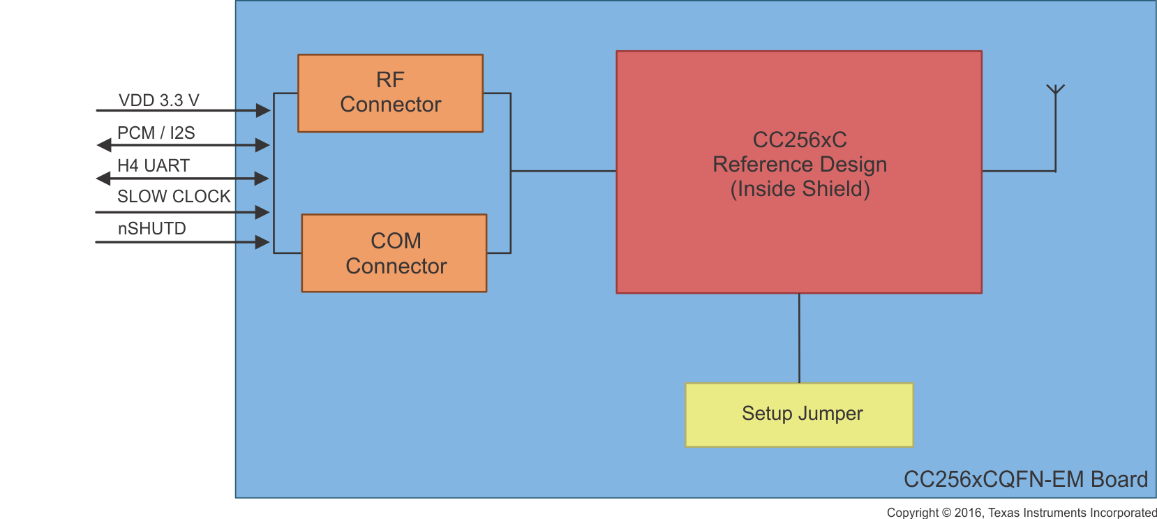
 CC256xCQFN-EM Block
                    Diagram Figure 3-1 CC256xCQFN-EM Block Diagram