TIDT238 July   2021 TL7700-SEP


  1. 1Description
  2. 2Test Prerequisites
    1. 2.1 Voltage and Current Requirements
    2. 2.2 Considerations
    3. 2.3 Dimensions
  3. 3Testing and Results
    1. 3.1 Efficiency Graphs
    2. 3.2 Efficiency Data
    3. 3.3 Thermal Images
    4. 3.4 EMI
  4. 4Waveforms
    1. 4.1 Switching
    2. 4.2 Output Voltage Ripple
    3. 4.3 Load Transients
    4. 4.4 Start-up Sequence

Output Voltage Ripple

Output voltage ripple was measured across a 0.1-µF ceramic capacitor placed across the output connector.

At full load the peak-to-peak ripple is less than 50 mV.
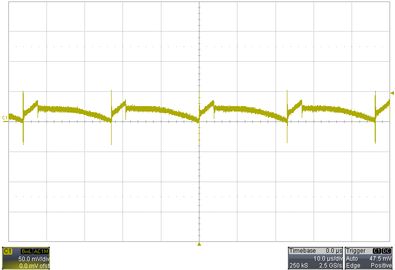
GUID-20210427-CA0I-7DWM-CQ9D-L6PSHBFC2Q6J-low.png Figure 4-2 Output Voltage Ripple