TIDT238 July 2021 TL7700-SEP
4.1 Switching
Switching behavior was measured across D3.
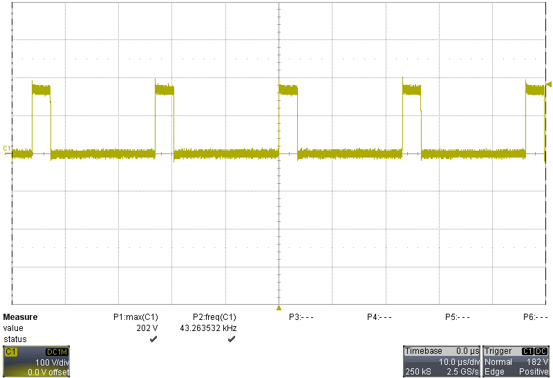
The max stress seen by the free-wheeling diode is 202-VDC with a 120-VAC input.
 Figure 4-1 Switch Node
TIDT238 July 2021 TL7700-SEP
Switching behavior was measured across D3.
The max stress seen by the free-wheeling diode is 202-VDC with a 120-VAC input.
 Figure 4-1 Switch Node