TIDUCL3 February 2017
- 1 Overview
- 2 Resources
- 3 Features
- 4 Applications
- 5 Design Images
- 6 System Overview
-
7 System Design Theory
- 7.1 PCB and Form Factor
- 7.2 Optimizing Board Performance Based on LED String Voltage and Current
- 7.3 Switching Frequency
- 7.4 Output Overvoltage Protection (OVP)
- 7.5 Current Monitoring (IMON)
- 7.6 Thermal Foldback
- 7.7 Clock Generation (PWM)
- 7.8 Onboard Supply and Setting Duty Cycle
- 7.9 Buffering, Averaging, and Filtering
- 7.10 Boost Converter
- 8 Getting Started Hardware
- 9 Testing and Results
- 10Design Files
- 11Related Documentation
- 12About the Author
7.8 Onboard Supply and Setting Duty Cycle
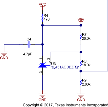
The supply for the TLC555-Q1 device, the OPA2377-Q1 op amp, as well as the reference voltage for setting the duty cycle is derived from the precision shunt regulator (0.5%) TL431-Q1 (see Figure 19). The device is supplied by the VCC (7.5 V) output of the TPS92691 device and regulates this voltage down to a precision 5 V (V5V) set by the resistors R7, R8, and R9. Additionally, the reference voltage for the op amp, which is used to set the duty cycle, is derived from this voltage that resistor divider R8 and R9 generate.
 Figure 19. TL431-Q1 Precision Voltage Generation