TIDUDO6B May 2019 – October 2020
- Description
- Resources
- Features
- Applications
- 5
- 1System Description
-
2System Overview
- 2.1 Block Diagram
- 2.2 Highlighted Products
- 2.3
System Design Theory and Design Considerations
- 2.3.1 AFE4900 and Power Supply
- 2.3.2 CC2640R2F Microcontroller
- 2.3.3 PPG Measurement
- 2.3.4 ECG Measurement
- 2.3.5 Selecting TX Supply (TX_SUP) Value for Driving LEDs
- 2.3.6 Generating TX Supply for Driving LEDs
- 2.3.7 Generating RX Supply for AFE4900
- 2.3.8 Generating I/O Supply
- 2.3.9 Battery Input and Reservoir Capacitors
- 2.3.10 Battery Life Calculations
- 2.3.11 External Memory
- 2.3.12 LED Indications
- 2.3.13 Connections Between Sensor Board and ECG Board
-
3Hardware, Software, Testing Requirements, and Test Results
- 3.1 Required Hardware and Software
- 3.2 Testing and Results
-
4Design Files
- 4.1 Schematics
- 4.2 Bill of Materials
- 4.3
PCB Layout Recommendations
- 4.3.1 Layout for Main Board
- 4.3.2 Connection From PDs to AFE
- 4.3.3 Connections From LEDs to AFE
- 4.3.4 Connections From ECG PADs to AFE
- 4.3.5 Connections Between BT and AFE
- 4.3.6 Connections Between BT Antenna and Chip
- 4.3.7 Boost Converter
- 4.3.8 Buck-Boost Converter
- 4.3.9 Layouts for PPG Sensor Boards
- 4.3.10 Layout for ECG Sensor Board
- 4.3.11 Layout Prints
- 4.4 Altium Project
- 4.5 Gerber Files
- 4.6 Assembly Drawings
- 5Software Files
- 6Related Documentation
- 7About the Authors
- Revision History
2.3.2 CC2640R2F Microcontroller
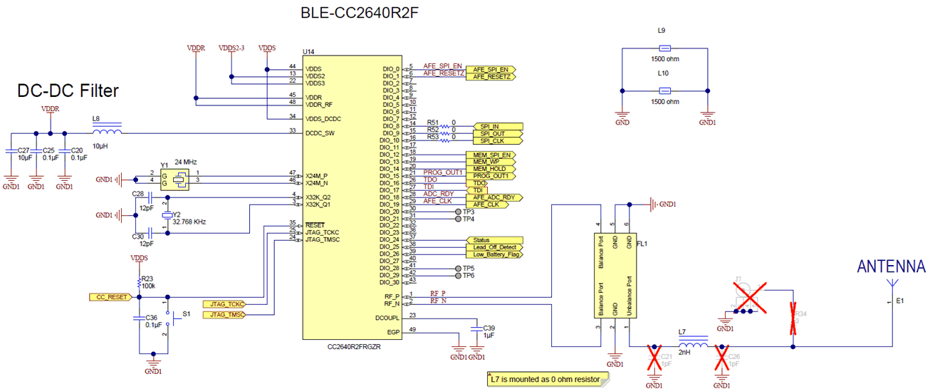
Figure 2-3 shows the schematic for configuring the CC2640R2F MCU.
 Figure 2-3 CC2640R2F MCU Schematic
The VDSS power supply for the MCU, 2.1 V, is derived using the TPS63036 device. The VDDR power supply is generated using the internal DC/DC of the CC2640R2F MCU, and L8, C20, C25, and C27 form the filter components for the same. Y1 is the 24-MHz, high-frequency, external clock and Y2 is the 32-kHz, low-frequency, external clock. The GPIO pins of the CC2640R2F MCU (DIO_0 to DIO_30) interface with different functions such as Memory interface lines, AFE4900 interface lines, SPI communication, LED drives, and so on.
The RF front end is used in differential-ended configurations with internal biasing. A Balun LFB182G45BG5D920 device is used for the RF front end and tuned for application. J7 is a connector for conducted RF measurements (if required). The antenna is a PCB antenna.
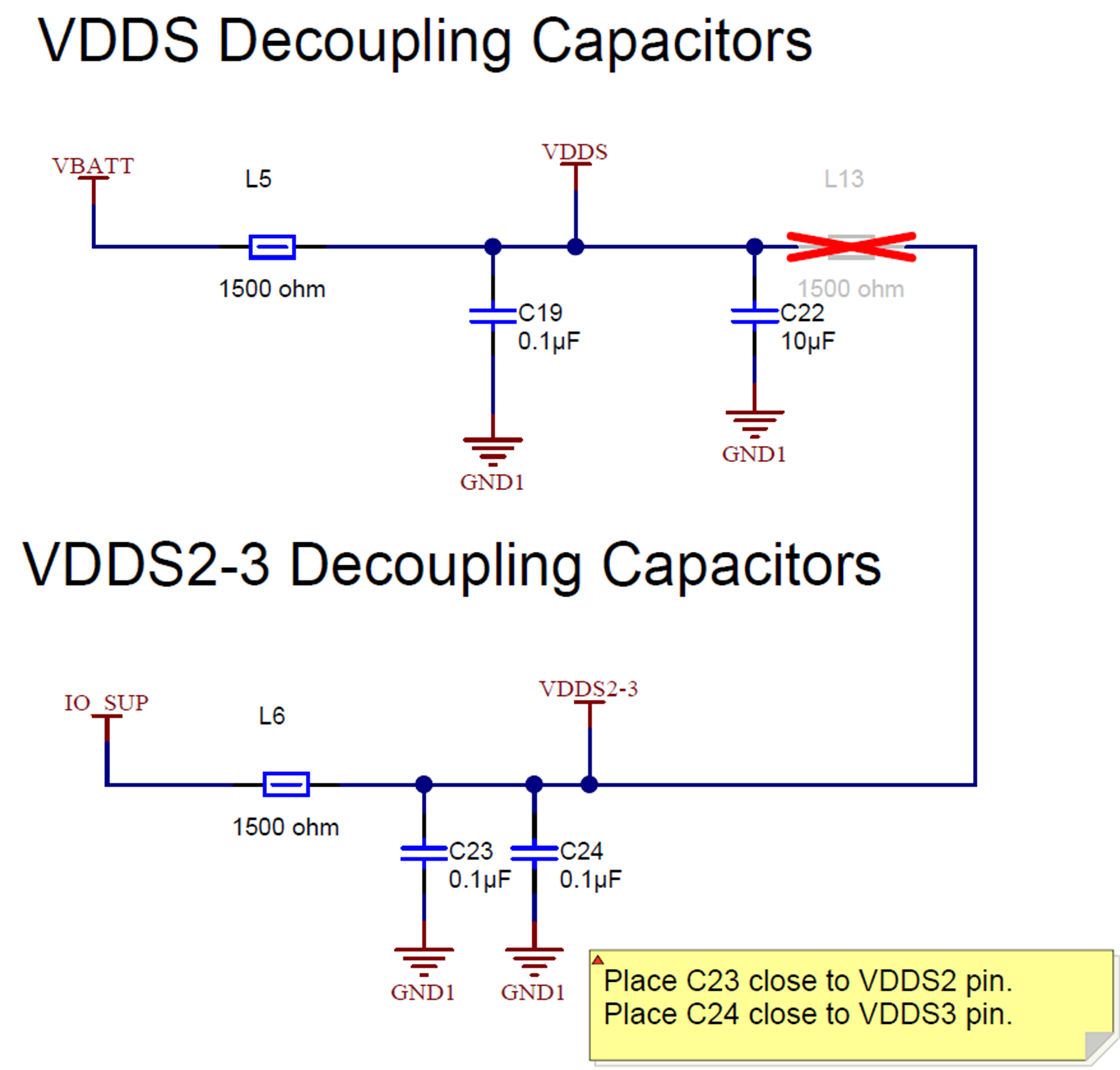
 Figure 2-4 Decoupling for CC2640R2F MCU
VBATT is connected to VDSS through L5 (a GHz noise-suppression chip ferrite bead), providing a low-noise supply to the MCU. C19 and C22 are the decoupling capacitors. A 2.1 V is connected to the VDDS2 and VDDS3 pins through L6 (a GHz noise-suppression chip ferrite bead), providing a low-noise supply to the MCU. C23 and C24 are the decoupling capacitors (see Figure 2-4).
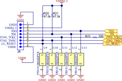
 Figure 2-5 MCU Programming Connector
The MCU is programmed using a JTAG connection, as shown in Figure 2-5. The connector inputs are protected by ESD diodes (TPD1E10B06DPYR) from Texas Instruments. The TPD1E10B06 device is a single-channel, ESD, TVS diode in a small 0402 package. This TVS protection product offers ±30-kV contact ESD, ±30-kV IEC air-gap protection, and an ESD clamp circuit, with a back-to-back TVS diode for bipolar or bidirectional signal support.