TIDUDO6B May 2019 – October 2020
- Description
- Resources
- Features
- Applications
- 5
- 1System Description
-
2System Overview
- 2.1 Block Diagram
- 2.2 Highlighted Products
- 2.3
System Design Theory and Design Considerations
- 2.3.1 AFE4900 and Power Supply
- 2.3.2 CC2640R2F Microcontroller
- 2.3.3 PPG Measurement
- 2.3.4 ECG Measurement
- 2.3.5 Selecting TX Supply (TX_SUP) Value for Driving LEDs
- 2.3.6 Generating TX Supply for Driving LEDs
- 2.3.7 Generating RX Supply for AFE4900
- 2.3.8 Generating I/O Supply
- 2.3.9 Battery Input and Reservoir Capacitors
- 2.3.10 Battery Life Calculations
- 2.3.11 External Memory
- 2.3.12 LED Indications
- 2.3.13 Connections Between Sensor Board and ECG Board
-
3Hardware, Software, Testing Requirements, and Test Results
- 3.1 Required Hardware and Software
- 3.2 Testing and Results
-
4Design Files
- 4.1 Schematics
- 4.2 Bill of Materials
- 4.3
PCB Layout Recommendations
- 4.3.1 Layout for Main Board
- 4.3.2 Connection From PDs to AFE
- 4.3.3 Connections From LEDs to AFE
- 4.3.4 Connections From ECG PADs to AFE
- 4.3.5 Connections Between BT and AFE
- 4.3.6 Connections Between BT Antenna and Chip
- 4.3.7 Boost Converter
- 4.3.8 Buck-Boost Converter
- 4.3.9 Layouts for PPG Sensor Boards
- 4.3.10 Layout for ECG Sensor Board
- 4.3.11 Layout Prints
- 4.4 Altium Project
- 4.5 Gerber Files
- 4.6 Assembly Drawings
- 5Software Files
- 6Related Documentation
- 7About the Authors
- Revision History
2.3.10.1 AFE4900 Current Consumption
The current consumption of the AFE4900 device depends on the sampling rate (for example, PTT mode at 1-kHz sampling rate for both ECG and PPG).
Typical specifications are at TA = 25°C; TX_SUP = 5 V, RX_SUP = 1.8 V (with CONTROL1 = 1.8 V to bypass internal LDOs), IO_SUP = 1.8 V, external clock mode with 32-kHz clock on CLK pin (period = tTE = 31.25 µs), the AFE operates with ULP mode enabled (ENABLE_ULP = 1); PPG: 1-kHz sampling rate, SAMP width of 3 × tTE, LED ON width of 4 × tTE, CF chosen such that there are 7-8 TIA time constants within the SAMP width, NUMAV = 1 (2 ADC averages), noise-reduction filter bandwidth set to 2.5 kHz, CIN = 100 pF (capacitor across the input pins to model the zero bias differential capacitance of the PD); ECG: 1-kHz sampling rate, INA gain of 12, chopper mode enabled (unless otherwise noted).
| PARAMETER | TEST CONDITIONS | MIN | TYP | MAX | UNIT | |
|---|---|---|---|---|---|---|
| CURRENT CONSUMPTION | ||||||
| RX_SUP current excluding switching current from I2C or SPI readout(5) | Low PRF PPG signal acquisition(3) | 50 | µA | |||
| High PRF ECG, PPG signal acquisition(4) | 600 | |||||
| Hardware power-down (PWDN) mode(2) | < 1 | |||||
| Software power-down (PDNAFE) mode(2) | 15 | |||||
| RX_SUP current resulting from switching current at I2C readout | At PRF of 50 Hz, readout with FIFO enabled with FIFO_PERIOD = 60, FIFO_NPHASE = 4(6) | 6 | µA | |||
| Power-down mode | 0 | |||||
| IO_SUP current | Low PRF, PPG signal acquisition(3) | 1 | µA | |||
| High PRF, ECG, PPG signal acquisition(3) | 1 | |||||
| Hardware power-down (PWDN) mode(2) | < 1 | |||||
| Software power-down (PDNAFE) mode(2) | < 1 | |||||
| TX_SUP current | Low PRF, PPG signal acquisition(3) | 4 | µA | |||
| High PRF, ECG, PPG signal acquisition(4) | 20 | |||||
| Hardware power-down (PWDN) mode(2)(1) | < 1 | |||||
| Software power-down (PDNAFE) mode(2)(1) | < 1 | |||||
| DIGITAL INPUTS | ||||||
| VIH | High-level input voltage | Digital inputs except CONTROL1, I2C_SPI_SEL | 0.9 × IO_SUP | IO_SUP | V | |
| CONTROL1 and I2C_SPI_SEL(7) | 0.85 × RX_SUP | RX_SUP | ||||
| VIL | Low-level input voltage | Digital inputs except CONTROL1, I2C_SPI_SEL | 0 | 0.1 × IO_SUP | V | |
| CONTROL1 and I2C_SPI_SEL(7) | 0 | 0.1 × RX_SUP | ||||
| DIGITAL OUTPUTS | ||||||
| VOH | High-level output voltage | IO_SUP | V | |||
| VOL | Low-level output voltage | 0 | V | |||
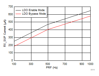
 Figure 2-19 Current Consumption for AFE4900 in LDO Enable Mode
The TX_SUP current is taken to be 3 mA at normal operating conditions (10% duty cycle for 100 mA) – worst case.
Over operating free-air temperature range (unless otherwise noted).
| PARAMETER(1)(2) | MIN | MAX | UNIT | |
|---|---|---|---|---|
| Supply voltage range | RX_SUP to GND LDO bypassed | –0.3 | 2.1 | V |
| RX_SUP to GND LDO enabled(3) | –0.3 | 4 | ||
| IO_SUP to GND | –0.3 | Min [4,(RX_SUP+0.3)] | ||
| TX_SUP to GND | –0.3 | 6 | ||
| Voltage applied to analog inputs | Max [–0.3, (GND – 0.3)] | Min [4.0, (RX_SUP + 0.3)] | V | |
| Voltage applied to digital inputs | Max [–0.3, (GND – 0.3)] | Min [4.0, (IO_SUP + 0.3)] | V | |
| Maximum duty cycle (cumulative): sum of all LED phase durations as a function of the total period | 50-mA LED current | 10% | ||
| 100-mA LED current | 3% | |||
| 200-mA LED current | 1% | |||
| Junction temperature, TJ | 105 | °C | ||
| Storage temperature, Tstg | –60 | 150 | °C | |
The RX_SUP and IO_SUP current are taken to be 700 µA (600 µA + 10 µA (I/O) + 50 µA (LDO enabled) + 40 µA (buffer)).