TIDUEX5 October   2020


  1.   Description
  2.   Resources
  3.   Applications
  4.   Features
  5.   5
  6. 1System Description
    1. 1.1 Key System Specifications
  7. 2System Overview
    1. 2.1 Block Diagram
    2. 2.2 Design Considerations
      1. 2.2.1 Ideal Diode Design Overview
      2. 2.2.2 Current Sensing Amplifier Design Overview
      3. 2.2.3 OR Gate Design Overview
      4. 2.2.4 MOSFET Selection
        1. 2.2.4.1 Blocking MOSFET
        2. 2.2.4.2 Hot-Swap MOSFET
      5. 2.2.5 TVS Input Diode Selection
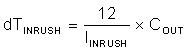
      6. 2.2.6 Inrush Current
    3. 2.3 Highlighted Products
      1. 2.3.1 LM74810-Q1
      2. 2.3.2 INA302-Q1
  8. 3Hardware, Software, Testing Requirements, and Test Results
    1. 3.1 Hardware Requirements
      1. 3.1.1 Getting Started
      2. 3.1.2 Testing and Results
        1. 3.1.2.1 Over-Voltage Protection Cut-Off Mode
        2. 3.1.2.2 Over-Voltage Protection Clamping-Mode
        3. 3.1.2.3 ISO7637-2 Pulse 1
        4. 3.1.2.4 Overcurrent Protection
        5. 3.1.2.5 Load Dump
        6. 3.1.2.6 Cold Crank, Warm Start, and Cold Start
          1. 3.1.2.6.1 Cold Crank
          2. 3.1.2.6.2 Warm Start
          3. 3.1.2.6.3 Cold Start
        7. 3.1.2.7 Standby Current
        8. 3.1.2.8 Currency Sense Accuracy
  9. 4Design and Documentation Support
    1. 4.1 Design Files
      1. 4.1.1 Schematics
      2. 4.1.2 BOM
    2. 4.2 Documentation Support
    3. 4.3 Support Resources
    4. 4.4 Trademarks

Inrush Current

Inrush limiting is achieved with LM74810-Q1 by placing a capacitor to slow down the HGATE voltage ramp during power up. The capacitor value required depends on the desired inrush current value as well as the amount of output capacitance. Equation 4 shows how to calculate the capacitor value needed. In the equation, is typically being 53 µA.

Equation 4. GUID-20200710-SS0I-J06Q-5N95-LGM948BVWSZL-low.gif

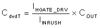
Duration of the inrush current can be calculated by Equation 5.

Equation 5. GUID-20200710-SS0I-48CX-DH4S-KCVBQJGK40QS-low.gif