TIDUEZ0A March 2021 – March 2022 TMS320F28P550SG , TMS320F28P550SJ , TMS320F28P559SG-Q1 , TMS320F28P559SJ-Q1
2.2.1 Three-Phase ANPC Inverter Architecture Overview
The basic architecture of the ANPC topology is shown in Figure 2-2.
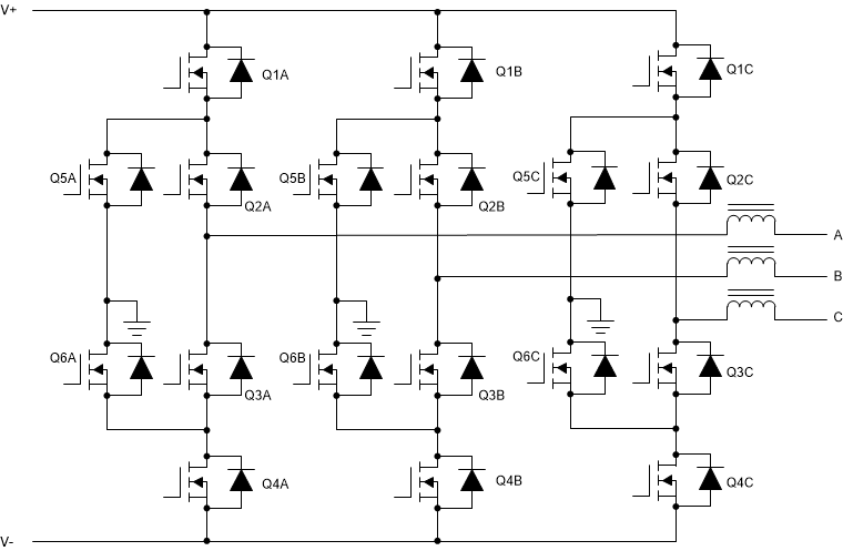 Figure 2-2 ANPC Three-Phase Inverter Architecture
To simplify the analysis, a single leg can be separated out as shown in Figure 2-3.
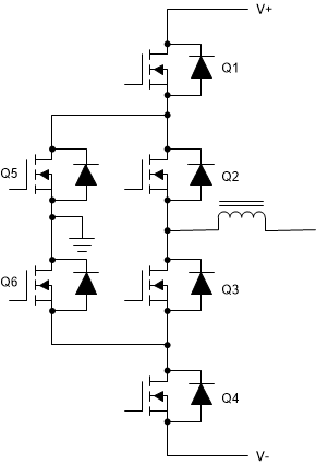 Figure 2-3 ANPC Single-Phase Inverter Leg
As can be seen, there are six switches in each phase. Though there can be various switching schemes to control this power stage, we selected a relatively simpler scheme to reduce complexity. The upper half of the circuit consisting of Q1, Q5 and Q2 is active during the positive half cycle and the lower half consisting of Q4, Q6 and Q3 is active during the negative half cycle. Q2 and Q3 are slow switches that connect the inductor to either the upper high frequency switching pair of Q1 & Q5 or Q4 & Q6 during positive and negative half cycles respectively. Each of the high frequency switching pairs is operated as a synchronous buck converter during their corresponding half cycles. The switching scheme is explained in detail in Figure 2-4 and Figure 2-5.
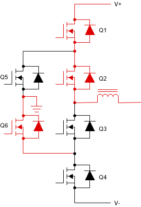 Figure 2-4 Inductor connected to V+
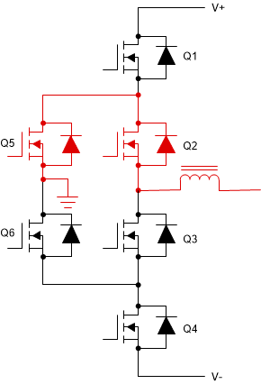 Figure 2-5 Inductor connected to N (+ve)
Figure 2-4 and Figure 2-5 show the operation of the circuit during the positive half cycle of this phase. The components in red are the ones that are conducting and those in black are the ones that are off. As can be seen Q2 remains on for the entire half cycle. When Q1 is on, the circuit is in active mode, establishing current flow from V+ to the inductor as in Figure 2-4. Since both Q1 and Q2 are on, the switching node of the inductor is connected to V+. Now, the switches Q3 and Q4 together have to withstand the full bus voltage. To avoid unequal distribution of the bus voltage among these devices (due to unequal device parasitics), Q6 also is kept on so that the central node gets connected to neutral, dividing the voltage equally between Q3 and Q4. When Q1 and Q6 are turned off together during the dead-time between the states shown in Figure 2-4 and Figure 2-5, the inductor current can only flow through the body diode of Q5 and Q2 (which stays on). During the freewheeling mode shown in Figure 2-5, Q5 acts as a synchronous diode, connecting the switching node of the inductor to neutral. Since the switches Q3 and Q4 have only half the bus voltage across them, it is not necessary to keep Q6 on for voltage balancing.
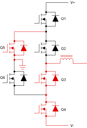 Figure 2-6 Inductor connected to V-
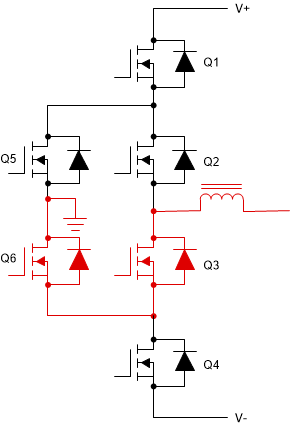 Figure 2-7 Inductor connected to N (-ve)
Similar to the operation during the positive half cycle, Figure 2-6 and Figure 2-7 illustrate the operation of the ANPC power stage during the negative half cycle. Q3 remains on for the entire duration of the negative half cycle.
Figure 2-6 shows the active mode operation in which the inductor gets connected to V- through Q4 and Q3. Similar to the operation during positive half cycle, Q5 also is kept on in this active mode operation to balance the voltage stress between Q1 and Q2. In freewheeling mode shown in Figure 2-7, the inductor current is maintained through Q6 and Q3, connecting the inductor switch node to neutral.