Packaging information
| Package | Pins VQFN (RSL) | 48 |
| Operating temperature range (°C) -40 to 105 |
| Package qty | Carrier 4,000 | LARGE T&R |
Features for the CDCDB800
- 8 LP-HCSL outputs with programmable integrated 85Ω (default) or 100Ω differential output terminations
- 8 hardware output enable (OE#) controls
- Additive phase jitter after PCIE Gen 7 filter: 11.3fs, RMS (maximum)
- Additive phase jitter after PCIE Gen 6 filter: 16.1fs, RMS (maximum)
- Additive phase jitter after PCIE Gen 5 filter: 25fs, RMS (maximum)
- Additive phase jitter after DB2000Q filter: 38fs, RMS (maximum)
- Supports Common Clock (CC) and Individual Reference (IR) architectures
- Spread spectrum-compatible
- Output-to-output skew: < 50ps
- Input-to-output delay: < 3ns
-
Fail-safe input
-
Programmable output slew rate control
- 3.3V core and IO supply voltages
- Hardware-controlled low power mode (PD#)
- Current consumption: 72mA maximum
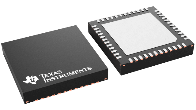
- 6mm × 6mm, 48-pin VQFN package
Description for the CDCDB800
The CDCDB800 is a 8-output LP-HCSL, DB800ZL-compliant, clock buffer capable of distributing the reference clock for PCIe Gen 1-7, QuickPath Interconnect (QPI), UPI, SAS, and SATA interfaces. The SMBus interface and eight output enable pins allow the configuration and control of all eight outputs individually. The CDCDB800 is a DB800ZL derivative buffer and meets or exceeds the system parameters in the DB800ZL specification. The device also meets or exceeds the parameters in the DB2000Q specification. The CDCDB800 is packaged in a 6mm × 6mm, 48-pin VQFN package.