Packaging information
| Package | Pins VQFN (RSL) | 48 |
| Operating temperature range (°C) -40 to 105 |
| Package qty | Carrier 4,000 | LARGE T&R |
Features for the CDCDB803
- 8 LP-HCSL outputs with programmable integrated 85-Ω (default) or 100-Ω differential output terminations
- 8 hardware output enable (OE#) controls
- Additive phase jitter after PCIE Gen 6 filter: 20 fs, RMS (maximum)
- Additive phase jitter after PCIE Gen 5 filter: 25 fs, RMS (maximum)
- Additive phase jitter after DB2000Q filter: 38 fs, RMS (maximum)
- Supports Common Clock (CC) and Individual Reference (IR) architectures
- Spread spectrum-compatible
- Output-to-output skew: < 50 ps
- Input-to-output delay: < 3 ns
-
Fail-safe input
-
Programmable output slew rate control
- 9 selectable SMBus addresses
- 3.3-V core and IO supply voltages
- Hardware-controlled low power mode (PD#)
- Current consumption: 72 mA maximum
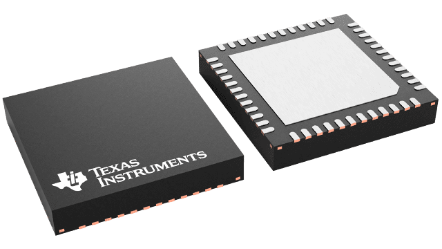
- 6-mm × 6-mm, 48-pin VQFN package
Description for the CDCDB803
The CDCDB803 is a 8-output LP-HCSL, DB800ZL-compliant, clock buffer capable of distributing the reference clock for PCIe Gen 1-6, QuickPath Interconnect (QPI), UPI, SAS, and SATA interfaces. The SMBus interface and eight output enable pins allow the configuration and control of all eight outputs individually. The CDCDB803 is a DB800ZL derivative buffer and meets or exceeds the system parameters in the DB800ZL specification. It also meets or exceeds the parameters in the DB2000Q specification. The CDCDB803 is packaged in a 6-mm × 6-mm, 48-pin VQFN package.