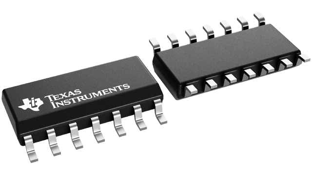
Packaging information
| Package | Pins SOIC (D) | 14 |
| Operating temperature range (°C) -40 to 85 |
| Package qty | Carrier 2,500 | LARGE T&R |
Features for the SN74ALVC08-EP
- Controlled Baseline
- One Assembly/Test Site, One Fabrication Site
- Enhanced Diminishing Manufacturing Sources (DMS) Support
- Enhanced Product-Change Notification
- Qualification Pedigree

- ESD Protection Exceeds 2000 V Per MIL-STD-883, Method 3015; Exceeds 200 V Using Machine Model (C = 200 pF, R = 0)
- Operates From 1.65 V to 3.6 V
- Max tpd of 2.9 ns at 3.3 V
- ±24-mA Output Drive at 3.3 V
- Latch-Up Performance Exceeds 250 mA Per JESD 17
 Component qualification in accordance with JEDEC and industry
standards to ensure reliable operation over an extended
temperature range. This includes, but is not limited to, Highly
Accelerated Stress Test (HAST) or biased 85/85, temperature
cycle, autoclave or unbiased HAST, electromigration, bond
intermetallic life, and mold compound life. Such qualification
testing should not be viewed as justifying use of this component
beyond specified performance and environmental limits.
Description for the SN74ALVC08-EP
The SN74ALVC08 quadruple 2-input positive-AND gate is designed for 1.65-V to 3.6-V VCC operation.
The device performs the Boolean function Y = A • B or Y (A\ + B\)\ in positive logic.
