Gehäuseinformationen
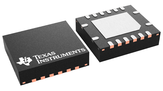
| Gehäuse | Pins VQFN (RGY) | 16 |
| Betriebstemperaturbereich (°C) -40 to 85 |
| Gehäusemenge | Träger 3.000 | LARGE T&R |
Merkmale von TXB0106
- 1.2 V to 3.6 V on A Port and 1.65 to 5.5 V on
B Port (VCCA≤ VCCB) - VCC Isolation Feature – If Either VCC Input Is at
GND, All Outputs Are in the High-Impedance
State - OE Input Circuit Referenced to VCCA
- Low-Power Consumption, 4 µA Max ICC
- Ioff Supports Partial-Power-Down Mode Operation
- Latch-Up Performance Exceeds 100 mA Per
JESD 78, Class II - ESD Protection Exceeds JESD 22
- A Port
- 2500 V Human Body Model (A114-B)
- 150 V Machine Model (A115-A)
- 1500 V Charged-Device Model (C101)
- B Port
- ±15 kV Human Body Model (A114-B)
- 150 V Machine Model (A115-A)
- 1500 V Charged-Device Model (C101)
- A Port
Beschreibung von TXB0106
This 6-bit noninverting translator uses two separate configurable power-supply rails. The A port is designed to track VCCA. VCCA accepts any supply voltage from 1.2 V to 3.6 V. The B port is designed to track VCCB. VCCB accepts any supply voltage from 1.65 V to 5.5 V. This allows for universal low-voltage bidirectional translation between any of the 1.2 V, 1.5 V, 1.8 V, 2.5 V, 3.3 V, and 5 V voltage nodes. VCCA should not exceed VCCB.
When the output-enable (OE) input is low, all outputs are placed in the high-impedance state.
The TXB0106 is designed so that the OE input circuit is supplied by VCCA.
This device is fully specified for partial-power-down applications using Ioff. The Ioff circuitry disables the outputs, preventing damaging current backflow through the device when it is powered down.
To ensure the high-impedance state during power up or power down, OE should be tied to GND through a pulldown resistor; the minimum value of the resistor is determined by the current-sourcing capability of the driver.