SBAS650C May   2014  – April 2021 AFE4403

PRODUCTION DATA  

  1. Features
  2. Applications
  3. Description
  4. Revision History
  5. Device Family Options
  6. Pin Configuration and Functions
  7. Specifications
    1. 7.1 Absolute Maximum Ratings
    2. 7.2 ESD Ratings
    3. 7.3 Recommended Operating Conditions
    4. 7.4 Thermal Information
    5. 7.5 Electrical Characteristics
    6. 7.6 Timing Requirements
    7. 7.7 Timing Requirements: Supply Ramp and Power-Down
    8. 7.8 Typical Characteristics
  8. Detailed Description
    1. 8.1 Overview
    2. 8.2 Functional Block Diagram
    3. 8.3 Feature Description
      1. 8.3.1 Receiver Channel
        1. 8.3.1.1 Receiver Front-End
        2. 8.3.1.2 Ambient Cancellation Scheme and Second Stage Gain Block
        3. 8.3.1.3 Receiver Control Signals
        4. 8.3.1.4 Receiver Timing
      2. 8.3.2 Clocking and Timing Signal Generation
      3. 8.3.3 Timer Module
        1. 8.3.3.1 Using the Timer Module
      4. 8.3.4 Receiver Subsystem Power Path
      5. 8.3.5 Transmit Section
        1. 8.3.5.1 Third LED Support
        2. 8.3.5.2 Transmitter Power Path
        3. 8.3.5.3 LED Power Reduction During Periods of Inactivity
        4. 8.3.5.4 LED Configurations
    4. 8.4 Device Functional Modes
      1. 8.4.1 ADC Operation and Averaging Module
        1. 8.4.1.1 Operation Without Averaging
        2. 8.4.1.2 Operation With Averaging
        3. 8.4.1.3 Dynamic Power-Down Mode
      2. 8.4.2 Diagnostics
        1. 8.4.2.1 Photodiode-Side Fault Detection
        2. 8.4.2.2 Transmitter-Side Fault Detection
        3. 8.4.2.3 Diagnostics Module
    5. 8.5 Programming
      1. 8.5.1 Serial Programming Interface
      2. 8.5.2 Reading and Writing Data
        1. 8.5.2.1 Writing Data
        2. 8.5.2.2 Reading Data
        3. 8.5.2.3 Multiple Data Reads and Writes
        4. 8.5.2.4 Register Initialization
        5. 8.5.2.5 AFE SPI Interface Design Considerations
    6. 8.6 Register Maps
      1. 8.6.1 AFE Register Map
      2. 8.6.2 AFE Register Description
  9. Application Information Disclaimer
    1. 9.1 Application Information
    2. 9.2 Typical Application
      1. 9.2.1 Design Requirements
      2. 9.2.2 Detailed Design Procedure
      3. 9.2.3 Application Curves
  10. 10Power Supply Recommendations
    1. 10.1 Power Consumption Considerations
  11. 11Layout
    1. 11.1 Layout Guidelines
    2. 11.2 Layout Example
  12. 12Device and Documentation Support
    1. 12.1 Trademarks
    2. 12.2 Electrostatic Discharge Caution
    3. 12.3 Glossary
  13. 13Mechanical, Packaging, and Orderable Information

Package Options

Mechanical Data (Package|Pins)
Thermal pad, mechanical data (Package|Pins)
Orderable Information

Reading Data

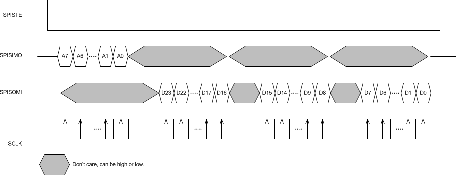
The SPI_READ register bit must be first set to 1 before reading from a register. The AFE4403 includes a mode where the contents of the internal registers can be read back on the SPISOMI pin. This mode may be useful as a diagnostic check to verify the serial interface communication between the external controller and the AFE. To enable this mode, first set the SPI_READ register bit using the SPI write command, as described in the Writing Data section. In the next command, specify the SPI register address with the desired content to be read. Within the same SPI command sequence, the AFE outputs the contents of the specified register on the SPISOMI pin. Figure 8-35 shows an SPI timing diagram for a single read operation. For multiple read and write cycles, refer to the Multiple Data Reads and Writes section.
GUID-5D05A7DF-796C-4E7A-BF13-E11D5973BB9B-low.gif
The SPI_READ register bit must be enabled before attempting a serial readout from the AFE.
Specify the register address of the content that must be readback on bits A[7:0].
The AFE outputs the contents of the specified register on the SPISOMI pin.
Figure 8-35 AFE SPI Read Timing Diagram