SBAS650C May   2014  – April 2021 AFE4403

PRODUCTION DATA  

  1. Features
  2. Applications
  3. Description
  4. Revision History
  5. Device Family Options
  6. Pin Configuration and Functions
  7. Specifications
    1. 7.1 Absolute Maximum Ratings
    2. 7.2 ESD Ratings
    3. 7.3 Recommended Operating Conditions
    4. 7.4 Thermal Information
    5. 7.5 Electrical Characteristics
    6. 7.6 Timing Requirements
    7. 7.7 Timing Requirements: Supply Ramp and Power-Down
    8. 7.8 Typical Characteristics
  8. Detailed Description
    1. 8.1 Overview
    2. 8.2 Functional Block Diagram
    3. 8.3 Feature Description
      1. 8.3.1 Receiver Channel
        1. 8.3.1.1 Receiver Front-End
        2. 8.3.1.2 Ambient Cancellation Scheme and Second Stage Gain Block
        3. 8.3.1.3 Receiver Control Signals
        4. 8.3.1.4 Receiver Timing
      2. 8.3.2 Clocking and Timing Signal Generation
      3. 8.3.3 Timer Module
        1. 8.3.3.1 Using the Timer Module
      4. 8.3.4 Receiver Subsystem Power Path
      5. 8.3.5 Transmit Section
        1. 8.3.5.1 Third LED Support
        2. 8.3.5.2 Transmitter Power Path
        3. 8.3.5.3 LED Power Reduction During Periods of Inactivity
        4. 8.3.5.4 LED Configurations
    4. 8.4 Device Functional Modes
      1. 8.4.1 ADC Operation and Averaging Module
        1. 8.4.1.1 Operation Without Averaging
        2. 8.4.1.2 Operation With Averaging
        3. 8.4.1.3 Dynamic Power-Down Mode
      2. 8.4.2 Diagnostics
        1. 8.4.2.1 Photodiode-Side Fault Detection
        2. 8.4.2.2 Transmitter-Side Fault Detection
        3. 8.4.2.3 Diagnostics Module
    5. 8.5 Programming
      1. 8.5.1 Serial Programming Interface
      2. 8.5.2 Reading and Writing Data
        1. 8.5.2.1 Writing Data
        2. 8.5.2.2 Reading Data
        3. 8.5.2.3 Multiple Data Reads and Writes
        4. 8.5.2.4 Register Initialization
        5. 8.5.2.5 AFE SPI Interface Design Considerations
    6. 8.6 Register Maps
      1. 8.6.1 AFE Register Map
      2. 8.6.2 AFE Register Description
  9. Application Information Disclaimer
    1. 9.1 Application Information
    2. 9.2 Typical Application
      1. 9.2.1 Design Requirements
      2. 9.2.2 Detailed Design Procedure
      3. 9.2.3 Application Curves
  10. 10Power Supply Recommendations
    1. 10.1 Power Consumption Considerations
  11. 11Layout
    1. 11.1 Layout Guidelines
    2. 11.2 Layout Example
  12. 12Device and Documentation Support
    1. 12.1 Trademarks
    2. 12.2 Electrostatic Discharge Caution
    3. 12.3 Glossary
  13. 13Mechanical, Packaging, and Orderable Information

Package Options

Mechanical Data (Package|Pins)
Thermal pad, mechanical data (Package|Pins)
Orderable Information

Description

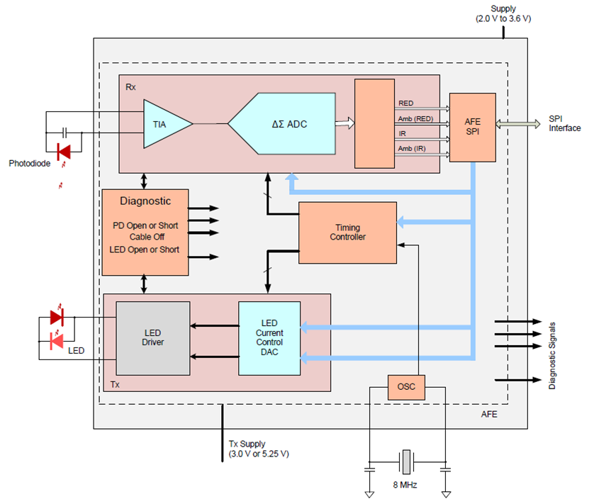
The AFE4403 is a fully-integrated analog front-end (AFE) ideally suited for pulse oximeter applications. The device consists of a low-noise receiver channel with an integrated analog-to-digital converter (ADC), an LED transmit section, and diagnostics for sensor and LED fault detection. The device is a very configurable timing controller. This flexibility enables the user to have complete control of the device timing characteristics. To ease clocking requirements and provide a low-jitter clock to the AFE4403, an oscillator is also integrated that functions from an external crystal. The device communicates to an external microcontroller or host processor using an SPI™ interface.

The device is a complete AFE solution packaged in a single, compact DSBGA-36 (3.07 mm × 3.07 mm × 0.5 mm) and is specified over the operating temperature range of –20°C to 70°C.

Device Information
PART NUMBERPACKAGE(1)BODY SIZE (NOM)
AFE4403 DSBGA (36) 3.07 mm × 3.07 mm
For all available packages, see the orderable addendum at the end of the datasheet.
GUID-0977EA10-E3E7-4287-8EA1-21E5E989D1A2-low.png Block Diagram